Recent Posts

Designing a keyboard from scratch - Part 1

23 minute read

Updates

  • The decoupling capacitor section has been corrected to add a missing capacitor. There are 5 VCC pins on the Atmega32U4 and I was missing one.
  • Thanks to Druz who discovered there was a mismatch between the reset button in the electronic schema and the footprint.

The article collection

This collection now contains the following articles:

  1. Part 1 (this one) - the electronic schema
  2. Part 2 - matrix & first steps of PCB layout
  3. Part 3 - routing the PCB

Preamble

I’ve been in the keyboard community for more than two years now and my keyboard collection is starting to fill up my shelves. It’s only recently that, as an engineer, I started to think about how keyboards were really working.

Some times ago, I got my hands on a 90s mint-condition Apple Extended Keyboard, some AEK keycaps and Alps SKCM switches. The idea I had, was to wait for a Group Buy to happen for an Alps based keyboard (like the ADK64) and then build a new keyboard with parts coming from old keyboards.

Alas, I missed all the nice Alps GB (ie the Lunar). Still I wanted to build a modern keyboard with those parts. One of the reasons is that I worked with such mechanical keyboards back in the 90s and I remember that their tactile feeling was among the best I’ve experienced.

So, an idea started to grow in my mind. What if I designed my own Alps based keyboard ? This way, I would be able to have the layout I want, instead of being forced in a 60% layout I’m not really fond of.

This series of articles will tell this adventure. My aim is to allow anyone to also start designing their own keyboards, piece by piece, but also understand how everything works.

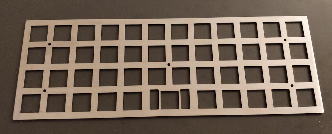
At the time of writing, I have validated the PCB rev0, almost finished designing the case and plate, but the keyboard itself is yet not finished.

In this episode, we’ll focus on beginning the electronic schema (outside the matrix). The very next episode will focus on the matrix, assigning footprints, etc. Then we’ll have at least one episode on the PCB design.
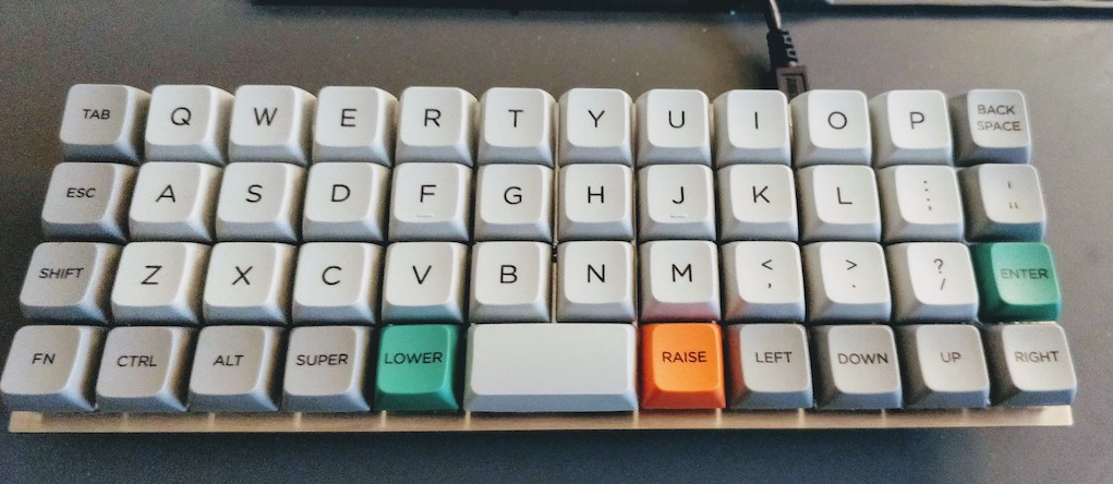
The keyboard

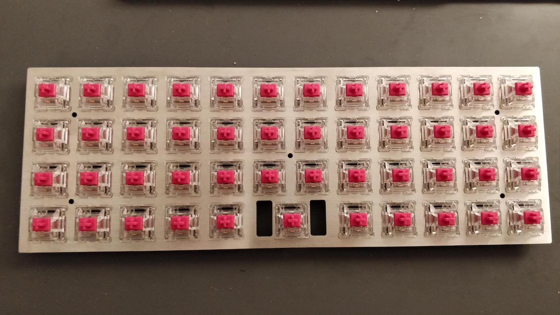
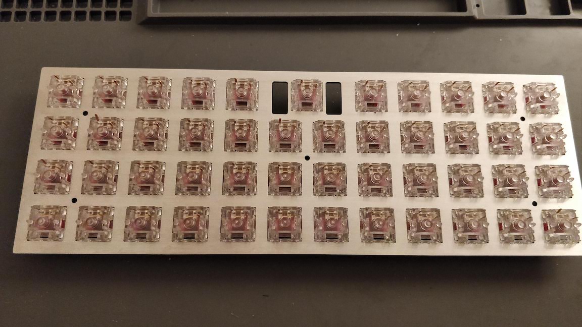
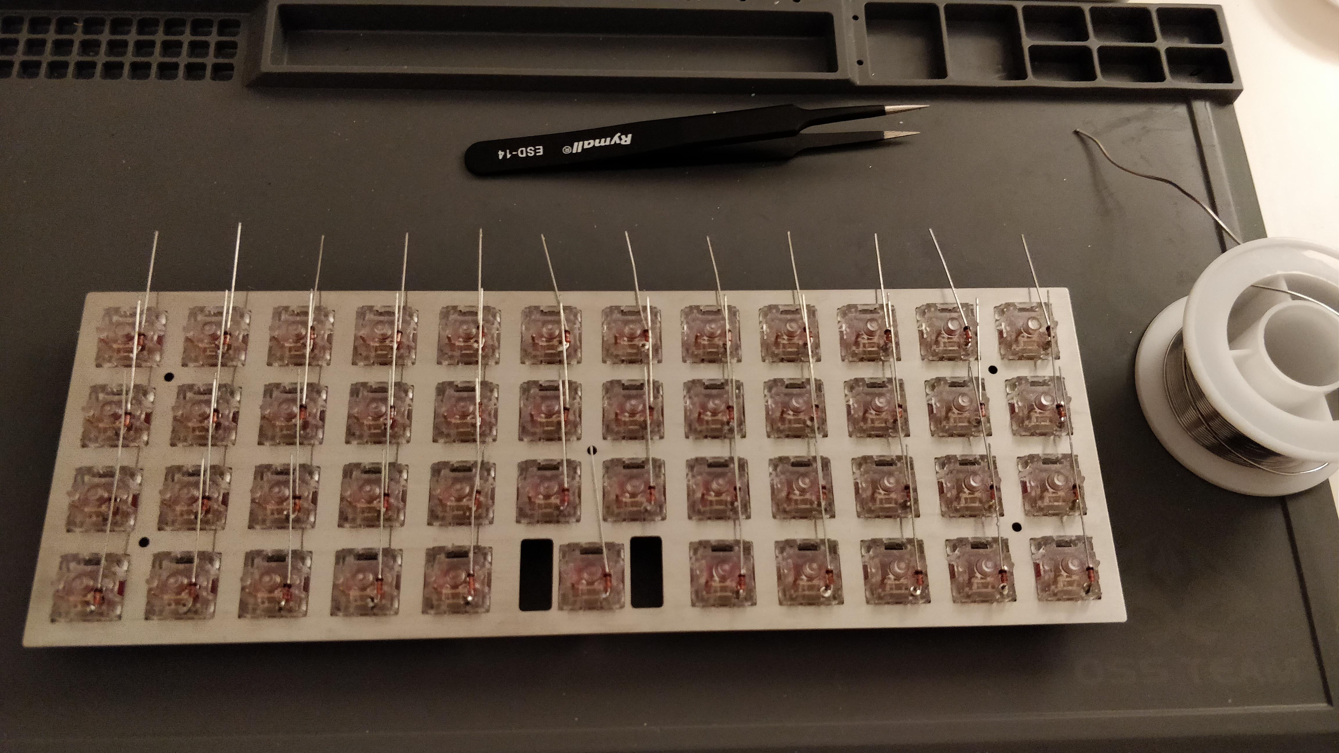
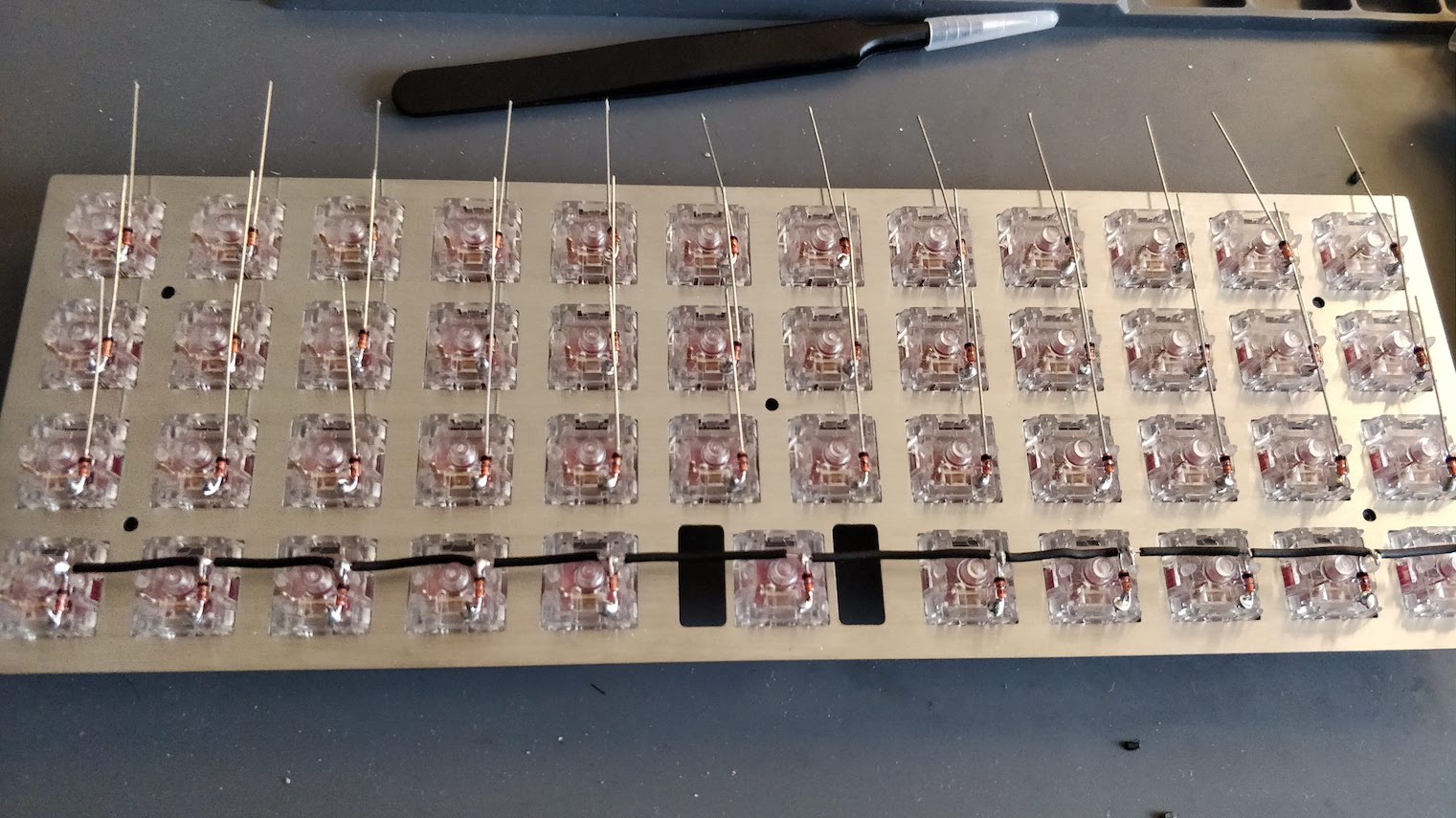
So I said earlier that I got some Salmon and Orange Alps SKCM switches that were desoldered from an existing 90s AEK. The Salmon switches are not in a very good condition (they would require cleaning at least), but the orange ones are. I also have 2 sets of AEK keys, one in Japanese and the other one in ANSI layout (qwerty US).

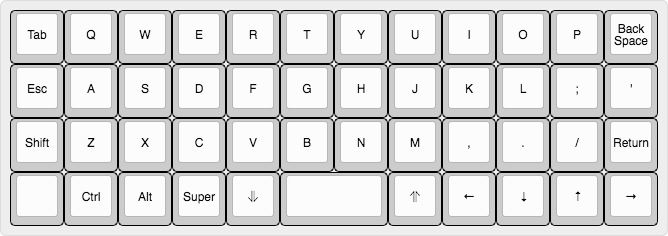
The aim is to build a 65% ANSI keyboard with the following layout:

AEK67 layout

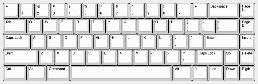
I codenamed this keyboard the AEK67 because there’s 67 keys in it, but I’m looking for a better name (any help would be very much appreciated on this front). You’ll notice that this layout is the same as the Lunar one. It also has the same issues:

  • it requires a 1.75u RSHIFT in row 3
  • it requires a 1u in row 4

The original AEK keyset doesn’t have those keys. There are possibilities of using a different key, for instance a Caps Lock, but it won’t have the right profile. The Lunar GB solved this issue by casting a specific 1.75u key in this profile, unfortunately I wasn’t able to get one. Well, we’ll see when the keyboard will be finished :)

Keyboard under the hood

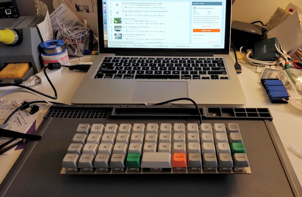
Unlike my previous experiment at building a handwired keyboard, this time the aim is to design a full-fledged keyboard, including a PCB and a real case.

Since I needed to start somewhere, and I already had some basic electronics knowledge from my engineering degree (25 year ago), I started by designing the electronic board.

I explained a bit how a keyboard works in the handwired build log, but let’s refresh our memories. A keyboard is the combination of:

  • keycaps (I’m covered)
  • switches (that’s OK, I got them)
  • a plate to secure the switches
  • a PCB on which the switches are soldered
  • a case
  • optionally a weight

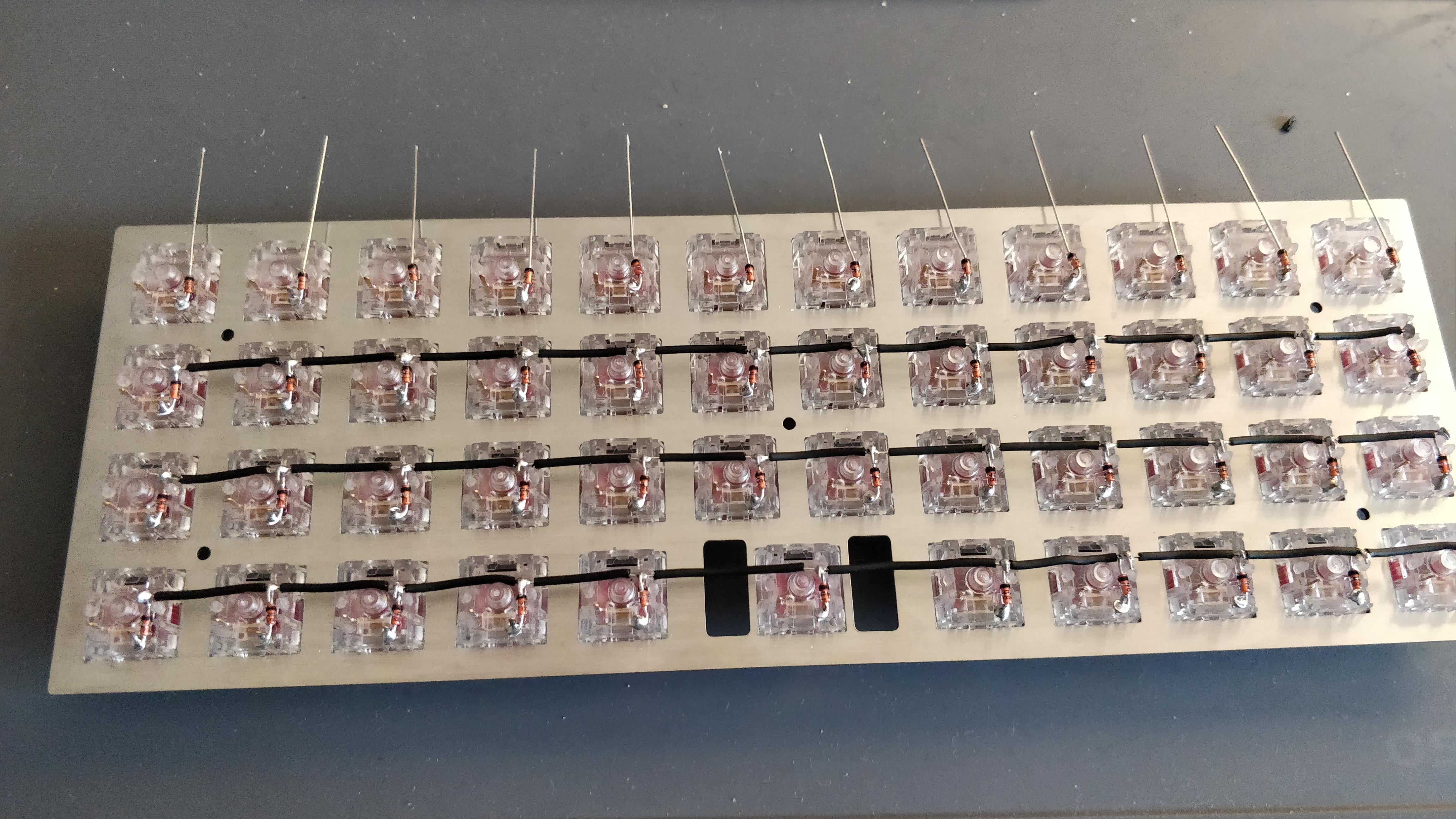
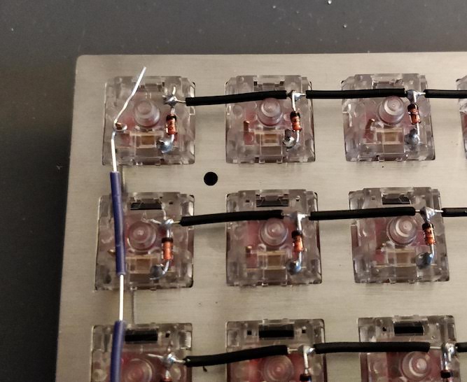
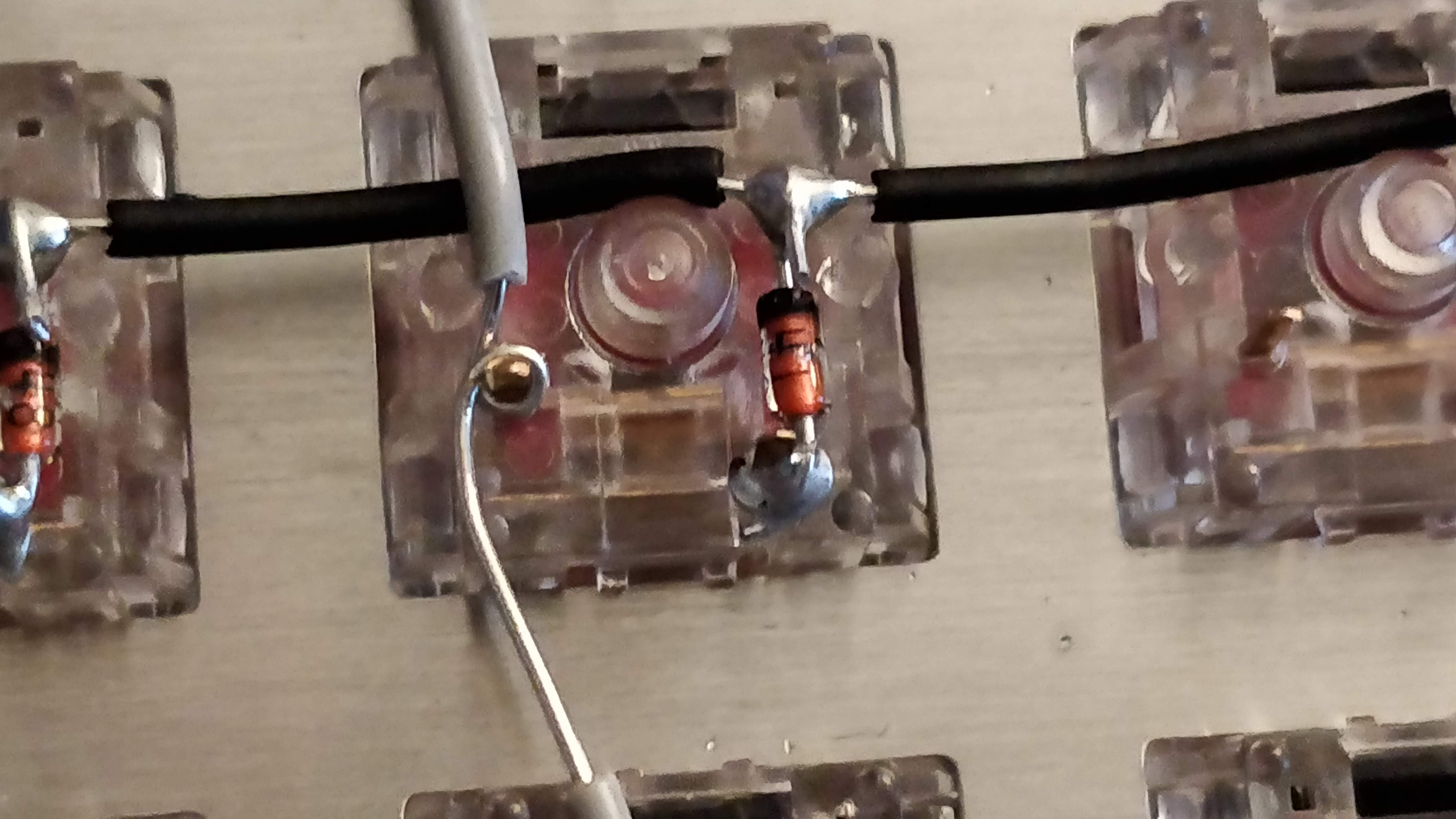
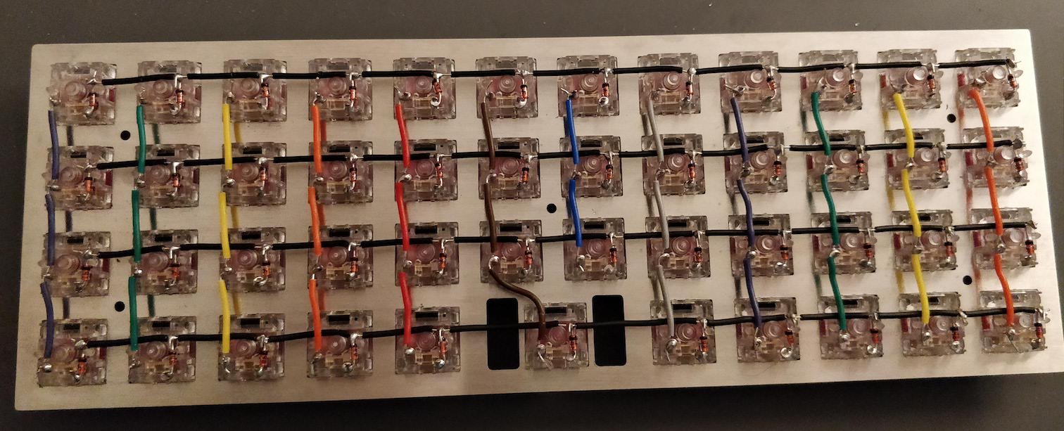
The PCB is the electronic board that converts key presses in commands that the computer can understand (that’s the HID protocol for USB). The PCB contains a micro controller (the MCU for short, it contains a CPU, a bit of RAM, flash memory and many I/O ports) and an array of switches (which form the matrix).

The switches are arranged in columns and rows to mimic the physical keys layout. At a very fast pace, the MCU will scan the matrix by providing a voltage on a given column, then the next one, etc and reading the lines.

If a key is depressed, the voltage will appear on the line of the pressed key when the MCU feeds the tension on its column, because the current will flow from the activated line to the row through the switch. The MCU deducts the key that has been depressed by looking at the rows and columns it is currently applying and reading the voltage.The MCU can then send the corresponding normalized key code on the USB wires to the computer (what the computer does is another story, sorry ;-)).

But there’s a problem: if one presses more than one key at a time, it is possible for the controller to register ghost keypresses. See the following schema of a conventional 4 switches matrix:

Ghosting Matrix

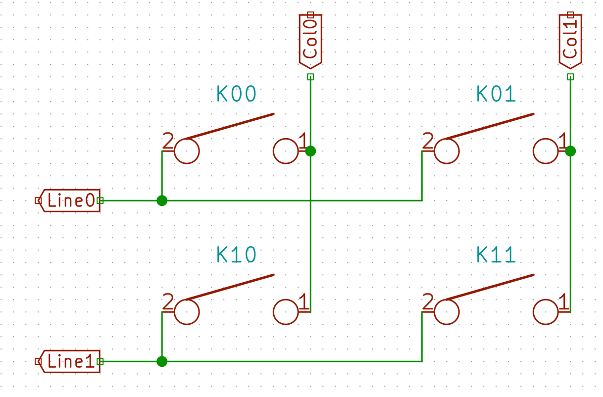
When the controller powers the Col0, and if K00, K01 and K11 are depressed simultaneously, the controller will see a tension on both Line0 and Line1, because the current will flow from Col0 to K00 pin 1, then pin 2 because the switch is closed, then to switch K01, then to switch K11, then to Line1. For the MCU it is as if all the switches have been pressed, instead of the 3 that were indeed depressed.

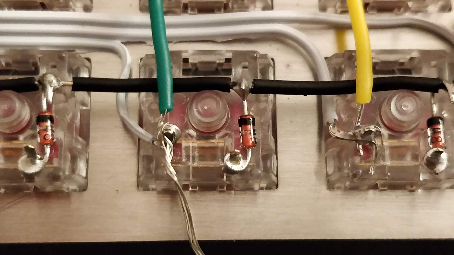
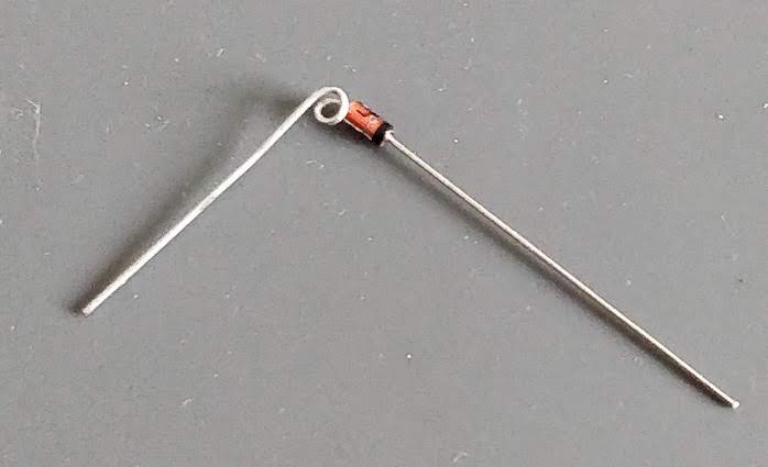
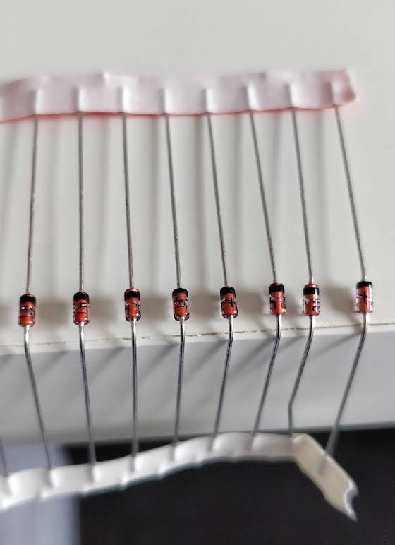
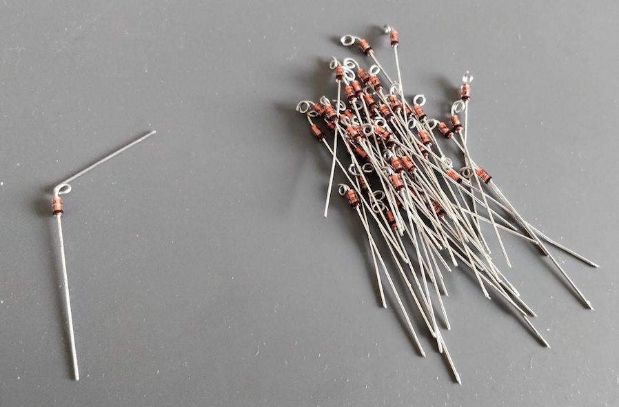
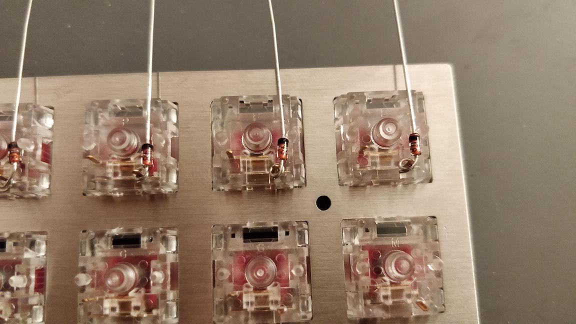
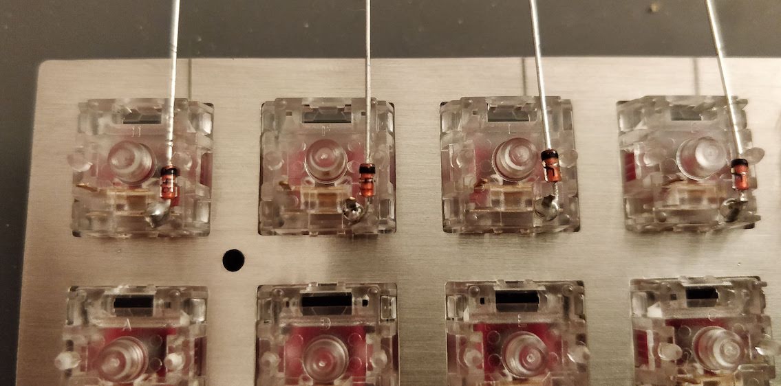
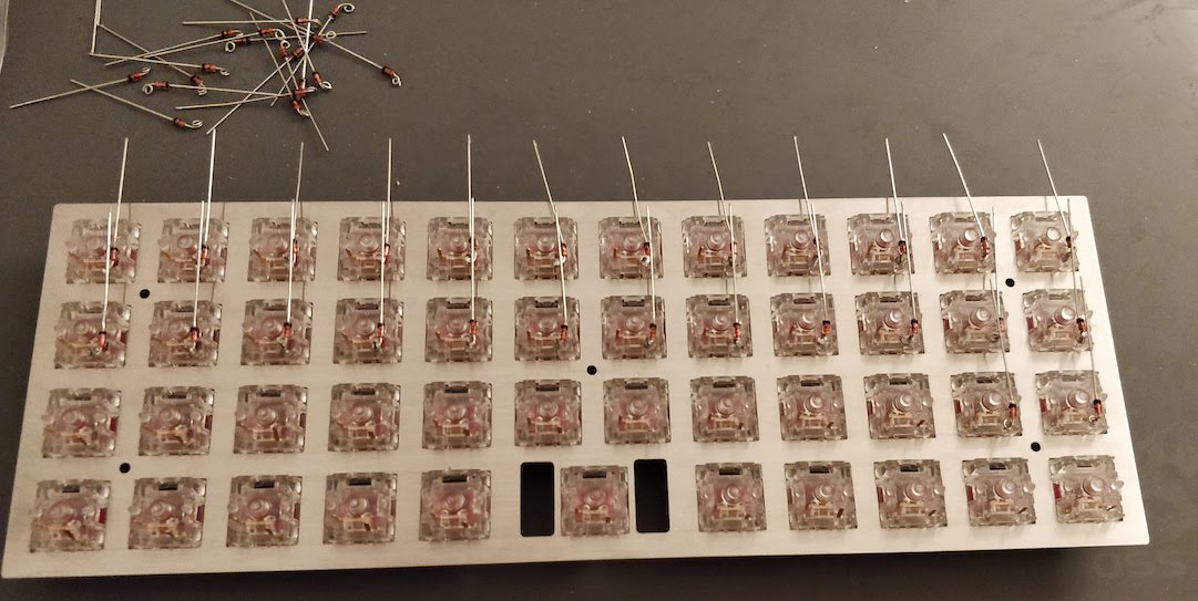
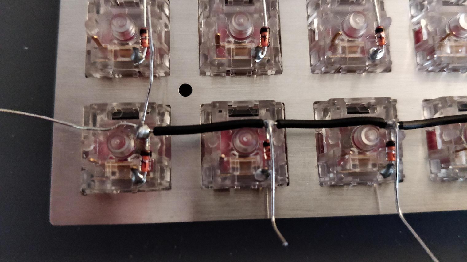
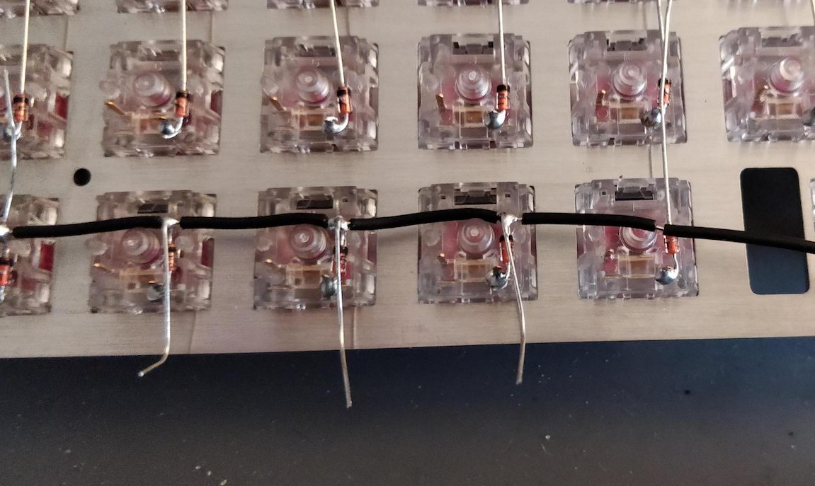
To prevent this we add diodes between the switch and the row it is connected to. Diodes are electronic components that prevent the current to flow in the reverse direction. The matrix becomes this:

Anti Ghosting Matrix

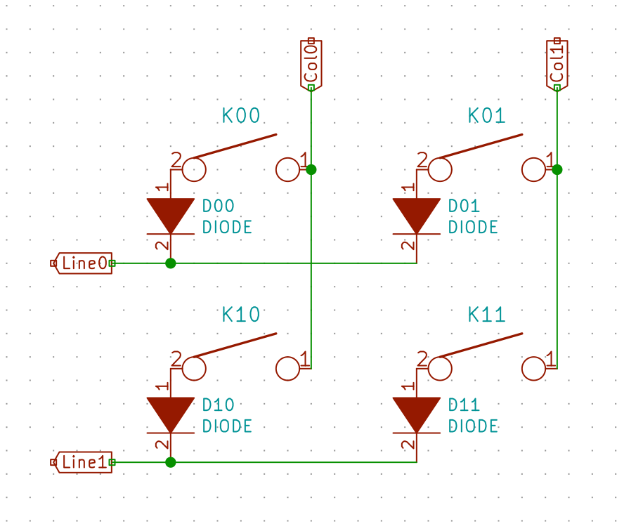
In the same hypothetical scenario as before, the current is prevented to flow back from K00 to K01 and from Line0 by the D01 diode. Thus when powering Col0, the controller will only see a tension on Line0, but not Line1. And when powering Col1 it will see a tension from Line0 and Line1, thus registering 3 key presses, as it should.

That being said, let’s start our work on the electronic schema.

Preparatory work

The last time I designed a PCB was during my engineering degree. And it was a long time ago. Things have changed nowadays. We now have open source software to design electronic schemas and PCB, no need to purchase a very expensive EDA software anymore, we have factories to build PCB at very low cost, etc.

Let’s start by installing the PCB design software: Kicad.

Since I was very rusty in this field, I needed a refresher on PCB design and keyboard inner workings. Hopefully, the keyboard community and especially ai03 has hosted a lot of very useful resources. The most important one is ai03’s awesome book on keyboard PCB design.

If you want to also start designing a PCB, I would suggest to read ai03’s tutorial (several times) and try to follow every steps. That’s a good way to get familiar with Kicad and its shortcuts.

One of his first advice is to work on the project under a git repository and to frequently commit. This is by far the most important advice I would recommend. It will allow you to come back in time if you fail something (and bonus point you can push to GitHub or any other central Git repository system to share your design).

So I started by creating a git repository, and added the keyboard kicad libraries I needed as git submodules:

Once done, fire Kicad and choose “File” -> “New Project”, and locate your git repository (make sure to uncheck working in a subdirectory). Kicad will have created 2 files:

  • the .sch file containing the electric schema
  • the .kicad_pcb file containing the PCB itself

We’re going to add our symbols and footprint libraries to the Kicad project.

Go to Preferences -> Manage Symbol Libraries, then add our 3 libraries as explained in this screenshot:

Kicad Symbol Libraries for this project

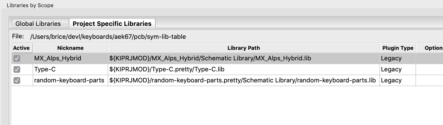
Next, go to Preferences -> Manage Footprint Libraries, and add our 3 footprints libraries (do not pay attention to the 2 extras libraries in my screenshot as I took it in a different project):

Kicad Footprints Libraries

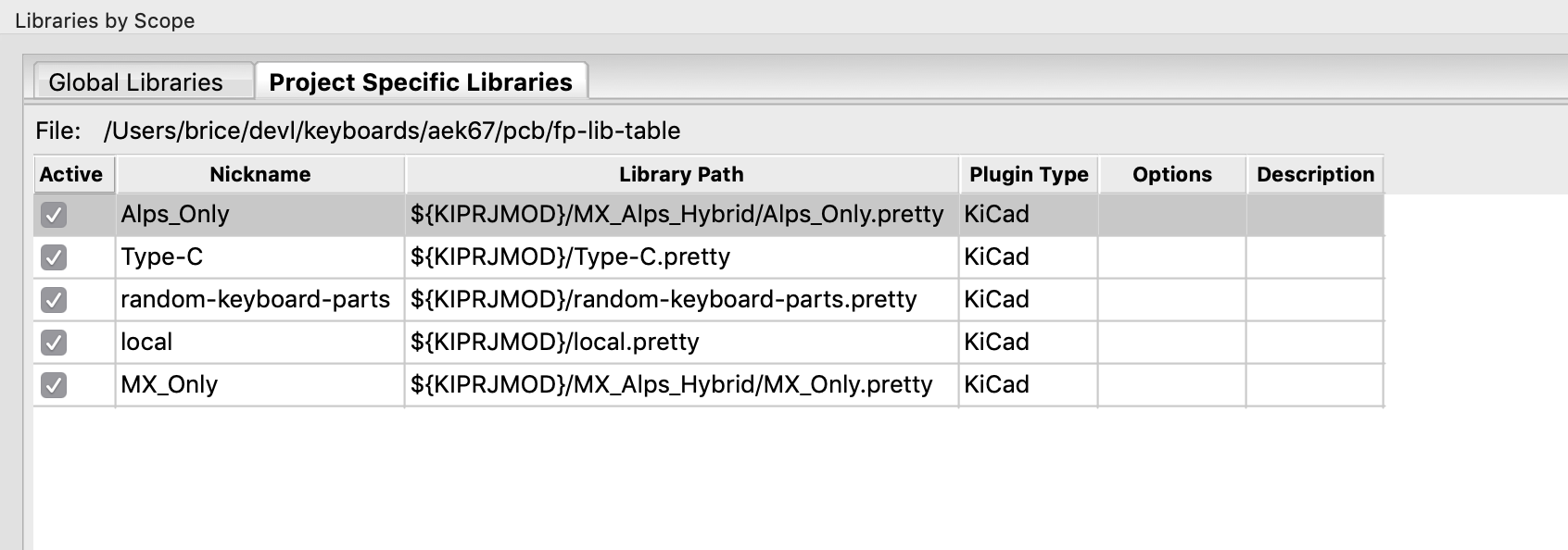
Note how I reference the libraries with the Kicad variable ${KIPRJMOD} which is a shorthand for the project location. This means that the project is relocatable (and anyone can check it out from GitHub without missing symbols problems).

Also note that I created a “local” footprints library in which we can put footprints we might need in this project but that are not in any specific library (or if we don’t want to import the whole library).

The electric schema

So the very first thing is to design the electric schema. In our case the electric schema has 3 distinct parts:

  • the MCU and it’s wiring
  • the USB port
  • the switch matrix

We’re going to use an Atmega32U4 as the MCU. This is the iconic MCU for keyboards, it is inexpensive, very well supported by QMK, has direct USB connectivity, comes with a factory loaded boot-loader and has enough I/O to drive a 65% matrix.

The design will use an USB-C connector and a protection circuit to prevent electro-static discharges to destroy the keyboard electronics.

To start working on the electronic schema, we double click on the .sch file in the Kicad project. This opens a blank page in the eeschema application.

Follow ai03’s guide to setup the schema grid to 50mils or 25mils.

If you work with a trackpad, make sure to check all 3 checkboxes in the Preferences Zoom & Pan section, otherwise using Kicad becomes very counter intuitive.

To properly use the schema editor, you need to first add a given component (shortcut a) and then wire it accordingly to the data-sheet (shortcut w to draw wire, k to stop wire at the mouse position).

Any action can be cancelled by pressing the Esc key.

To copy an element use the shortcut c while the mouse pointer is on a component and move it (it will be very handy for switches). The shortcut g moves with the wire attached. And finally, you have to know the shortcut e to edit any component characteristic (this is very useful), r to rotate and y to flip a component.

I need to introduce here two notions:

  • Labels: those are small text labels that you can attach to wires or pins to give them a name. All the wires that have the same labels are connected together without having to wire them physically in the schema.
  • Power symbols: Kicad will automatically wire power symbols of the same name together on a power net. This is especially useful for the GND and +5V symbols, because those are virtually needed everywhere and we don’t want to clutter our schema with such wires.

To place a power symbol, just press p and open the ‘power’ submenu, scroll down to either +5V or GND, then click on the schema to place the symbol, use r to rotate it as you want.

By setting the grid to 50mils, the mouse pointer will snap from point grid to point grid. Every component will be laid out on this grid, and IC pins will also be aligned on such a grid. This way you make sure wires will be connected correctly to the pins of the component without having to precisely aim to the pins. If you were to use a smaller grid, you’d do a lot of small misalignment and some pins would end up not connected.

Grid alignment

The MCU schema

The first thing to do is to add the Atmega32U4 symbol, by pressing the a key, then type Atmega32 in the component search window:

Adding the Atmega32U4

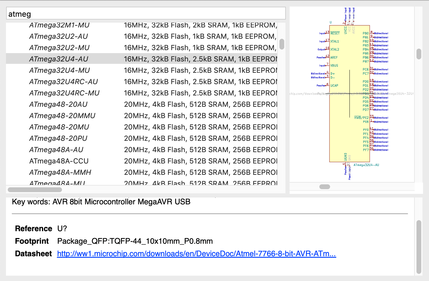
Let’s chose the official Kicad symbol for the Atmega32U4-AU. The AU package is a hand-solderable TQFP format (an IC with apparent pins, unlike the MU variant which is a QFN package where the pins are below making it difficult to solder with a standard solder iron).

Paste the MCU in the grid on the right part of the schema (but anywhere would work).

The MCU is easy to wire, and well explained in ai03’s guide, but to recap:
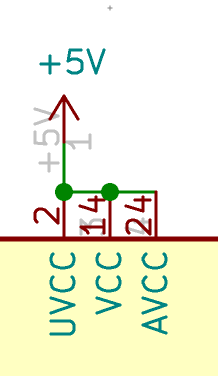
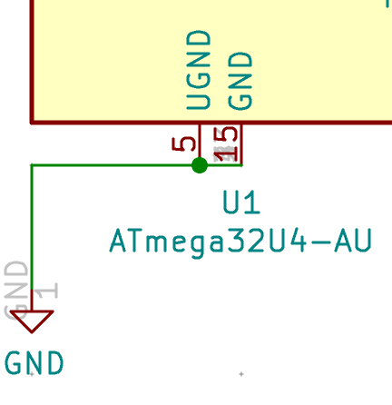
  • VCC, AVCC, UVCC should be connected to the +5V power symbol.
  • VBUS should also be connected to the +5V. VBUS is used by the MCU to monitor if it is connected or disconnected to/from the USB port. The Atmega32U4 data-sheets requires it to connect to a 10µF capacitance (see below).
  • GND and UGND should be connected to the GND power symbol
  • most of the pins will be left unconnected for the moment, as they’ll be hooked to the matrix rows and columns later

This gives this:

VCC

GND

The MCU can work without a clock, but it’s way better to provide it a real external clock. The external clock is a crystal oscillator (or resonator). It is a specific component that produces a square signal at 16 MHz (for our case, otherwise there are crystals for a lot of different frequencies). The MCU is using this clock to sequence instructions execution and other internal functions. When powered with +5V the Atmega32U4 can run at 16 MHz.

For the moment it is enough to add Global Labels to the pins. I’ll cover the crystal circuit a bit later:

XTAL

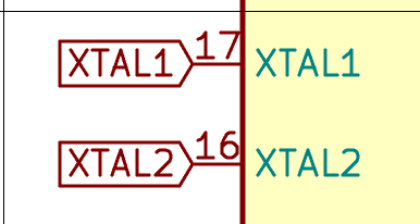
To add a label, press the Ctrl-H key and type it’s name (XTAL1), then place it onto the XTAL1 pin. Do the same with XTAL2. You might need to rotate the label either during creation or afterward (with r).

Let’s do the same with the D+/D- and RESET pins.

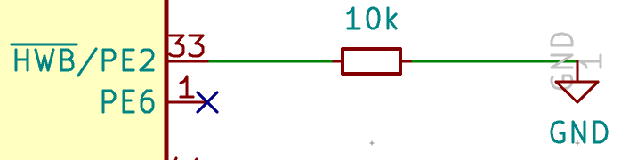
The next pin to wire is HWB. HWB is forced to GND with a pull down to make sure the MCU will boot with the boot-loader (refer to the data-sheet for more details). Create a R_small symbol for the resistor (we’ll use R_small symbols for all other resistors), then wire it like this:

HWB

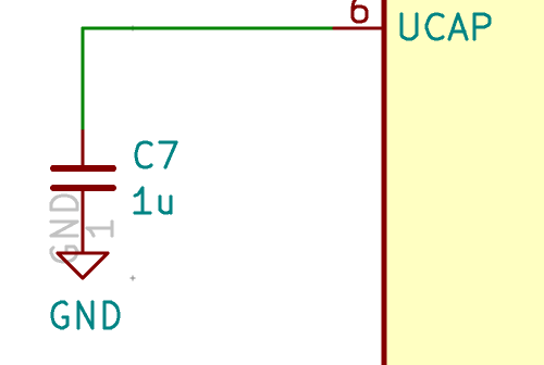
The UCAP is the internal USB pins voltage regulator, it has to be connected to a 1µF capacitor as instructed by the Atmega32U4 data-sheet. Use a C_small symbol for the capacitor (and all capacitors going forward)

UCAP

AREF doesn’t need to be wired, we’re going to mark it with a cross by pressing q and clicking on the pin. AREF (and AVCC FWIW) is used when doing analog signaling which we’re not going to do in our keyboard.
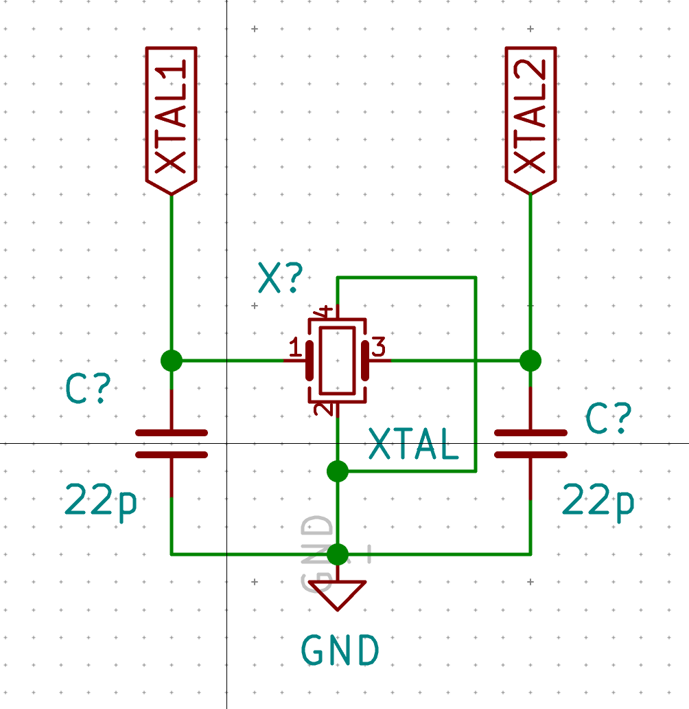
Hooking the clock

The very next step is to design the clock that drives the MCU and which will hook to the XTAL1 and XTAL2 labels.

The Atmega AN2519 tech-note gives a recommended design and equations to compute the capacitance values. Spoiler alert: the capacitor value is 22pF.

Place a Crystal_GND24_small on the grid close to the MCU. Then wire it like this:

Crystal Circuit

Every component on Kicad has several properties. Among them, we find two important ones:

  • the reference which is usually some letters followed by a number. It uniquely identifies a component on the schema
  • the value can be anything. For passive components it is usually their values (in ohms for resistor, farads for capacitance, etc) or the component name for ICs.

The reference isn’t attributed when you add a new component to the schema, it contains one or more ?. There is an operation in Kicad that allows to automatically assign references to all the components (we’ll use it soon). This is necessary to be able to create a PCB or run the Electric Design Rule Checker, etc.

To edit the component values and reference, you can press e while hovering the mouse pointer on the symbol. This allows to edit all facets of a given component, including its reference, value, but also it’s symbol and footprint. There are shortcuts to edit the value (v) or the reference (u) directly.

It is possible to move the reference or value label of a component by pressing m while the mouse is over the component. It’s what I did in the crystal schema so that values and references are not colliding with any wires.
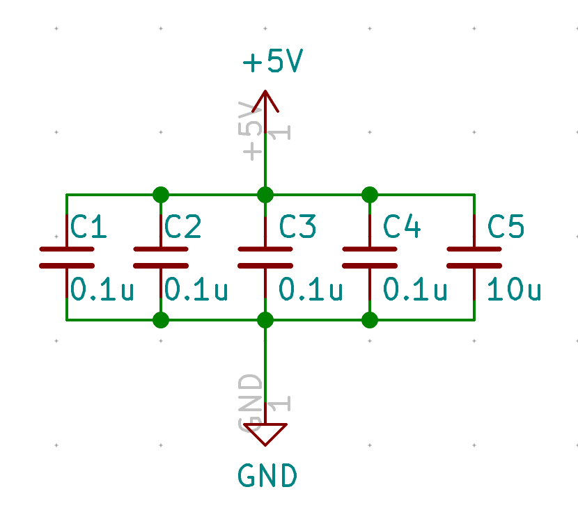
Power decoupling

The Atmega32U4 data-sheet recommends every +5V pins of the MCU to have decoupling capacitors. The decoupling capacitors play an important role for an active IC. If the component starts to draw current while doing its work, the voltage of the power source will drop, which could be problematic for the component itself but also for all other components powered by the same source (this creates noise on the power line).

To prevent this, we add decoupling capacitors on each power pin of the IC. Those decoupling capacitors will act as local energy storage. When the IC begins to consume energy the capacitors will be able to fulfill it without too much adverse effect on the power source. When the component doesn’t consume energy the decoupling capacitors refills gradually becoming ready for the next serve.

The AN2519 tech notes indicates that every VCC pins of the MCU should be decoupled by a 100nF (or 0.1µF) capacitor.

To be effective, the capacitor must be placed as close as possible from the MCU on the final PCB. Note that there are 4 VCC pins on the Atmega32U4 (2 AVCC, UVCC and 2 x VCC), so ideally we would need 5 100nF capacitor and one 10μF for VBUS. In practice, we can share the 10μF capacitor for both VBUS and UVCC and dispatch the 4 100nF to the other vcc pins.

To prevent cluttering the electronic schema, as ai03 suggests, I’ve placed those decoupling capacitors altogether in the schema.

Start by placing a capacitor, then use the c command to copy and move the next capacitor until you’ve placed all. Then wire them accordingly to this schema:

Decoupling Capacitors

ISP header

In case of catastrophic failure, it might be necessary to reprogram the Atmega32U4. In this case (for instance if we lost the DFU boot-loader), we can’t use the USB port to do that. We need to access the Serial Peripheral Interface (SPI) programming interface, and use the ISP programming mode.

To do this, we’re going to include on the PCB a 6 pins header with the SPI signals ready:

ISP header

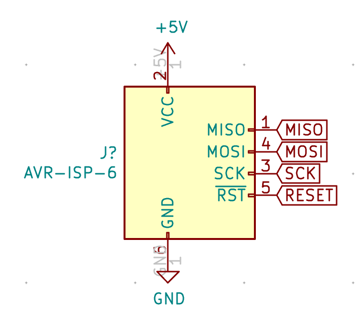
And associate it with the corresponding pins on the MCU:

SPI Pins

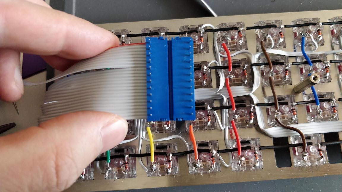
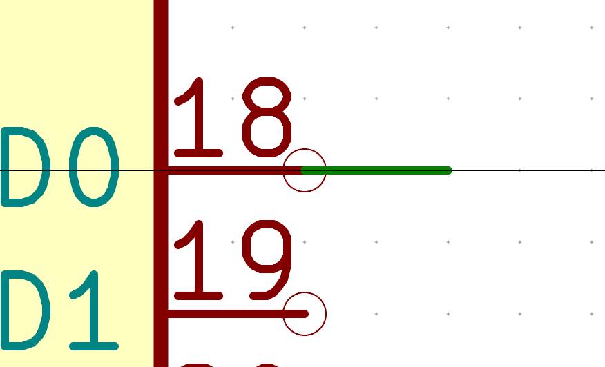
Notice that those 3 signals consume 3 general I/O pins which could be used for connecting the matrix. Since the matrix has 15 rows and 5 lines, it requires 20 I/O pins on the MCU. The MCU has thus enough available I/O pins. However if that wasn’t the case (for instance we might want to dedicate pins to RGB LEDs or backlighting or have a larger matrix), then it is very possible to share the ISP pins with the matrix. During ISP programming those matrix lines won’t be in use and during the keyboard use, the ISP pins won’t be in use. There are alternative matrix configurations to overcome a limited number of pins. Among them, you can double the number of rows and use the same “electrical” column for two consecutive physical columns. Another alternative is called Charlieplexing

Reset circuit

The keyboards needs to be flashed with a firmware (we’ll use the ubiquitous and opensource QMK).

The first time the Atmega32U4 boots, it will enter DFU mode because there’s no firmware loaded in the chip. The good thing with those MCU is that it is possible to flash them through the USB port and a program on the computer (for instance QMK Toolbox).

But, once done, if for any reason you need to update the firmware, there’s no way to make the firmware enter the DFU mode anymore (unless you included a RESET key combination in the keymap).

Hopefully, the MCU supports a way to perform an external reset, as the data-sheet explains: “The MCU is reset when a low level is present on the RESET pin for longer than the minimum pulse length.”

That means we can attach a push button to the reset pin to trigger a reset. But the tech notes also states: “The reset line has an internal pull-up resistor, but if the environment is noisy it can be insufficient and reset can therefore occur sporadically”. We don’t want to risk spurious reset, so we also need to add a pull-up resistor.

The AN2519 recommended design is the following one:

AN2519 recommended RESET circuit design

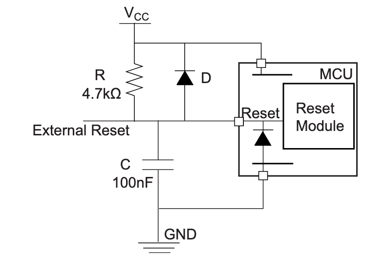
The tech-note recommended design adds a filtering capacitor to prevent noise in very noisy environments. I don’t think this keyboard will be used in such environments, we’re going to skip it (that’s one component less to solder, yay!).

The tech-note next paragraph adds the recommended design for a reset push button (this is to be combined with the):

AN2519 recommended RESET button

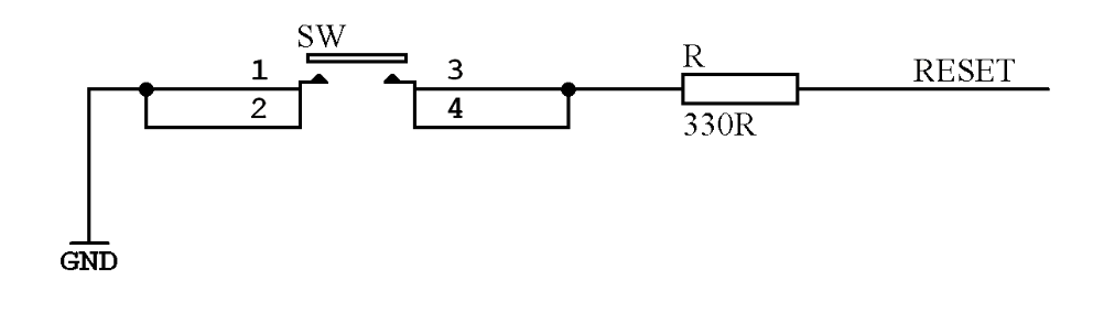
The 330 ohm resistor in series is to prevent a high current to form when shorting the capacitor at the moment the push button is pressed. This in turn would produce a high voltage on the RESET pin of the Atmega32u4 which could destroy it. Since we won’t use the capacitor, we don’t need this resistor altogether.

There’s no need to debounce the push button, because we really don’t care if we ever do multiple resets in a row when it is depressed.

There’s the question of the ESD protection diode parallel to the pull-up resistor. Since we don’t need His-Voltage/Parallel Programming (HVPP) for a keyboard (we’re going to do only USB and ISP flashing), the diode could be needed (otherwise it would prevent getting the 11V-15V needed on the RESET pin to trigger HVPP).

The ESD protection diode is just a standard diode (some recommend a Zener diode there). It protects from any electrostatic discharge damage. During the discharge, the external reset voltage is greater than 5.7V (Vcc 5V + 0.7V for the diode conduction), and the diode then conducts all the current toward the +5V source, thus protecting the RESET pin from the discharge current.

The diode has no interest for ESD protection if we only allow to reset with a push button (our case), but it might be of interest if we allow an external signal to trigger the reset. However the keyboard ISP header is for use only in case of emergency and will be hidden and protected in the keyboard case so the risk of ESD is quite negligible. I think it can be safe to remove this diode from the design.

Most open-source keyboard designs don’t have this diode either, probably for the same reason. To be noted that most of the Atmega32U4-based arduino board out-there don’t have the diode either.

For the real reset button I’m going to use a small SMD button like the RS-187R05A2-DS MT RT or the Alps SKQGAFE010.

The schematic of those buttons shows that there are 4 pins, each pair of pins connected horizontally. There’s no such symbol in Kicad yet. I could use a basic SW_PUSH with the alps footprint for instance and that would work fine. But I can also show you how to create your own symbol.

Let’s open the symbol editor from the Kicad main window. First I’ll create the local library (which has already been added to Kicad earlier). Then in this library, I’m creating the SW_SKQG symbol like this:

SW_SKQG

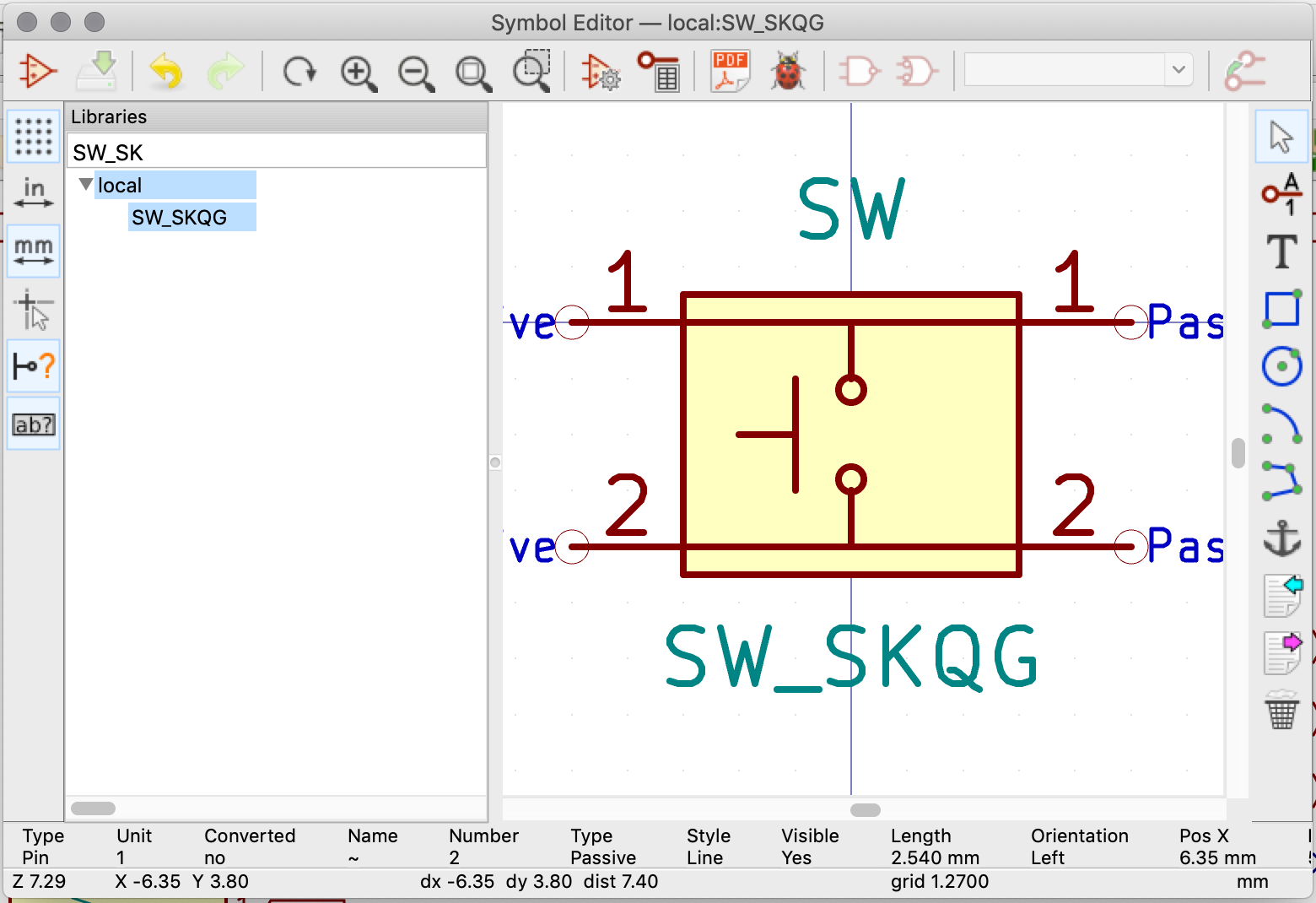
It’s composed of a rectangle, 4 pins labelled 1 & 2 and a few polylines and circles: nothing very complicated. Make sure to keep using the 50 mil grid settings to place the various pins, otherwise it will be difficult to connect the symbol in the schematic. Once done, save the symbol, it is ready to be used in the schematic:

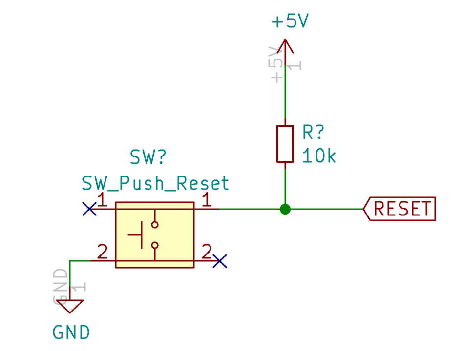
So, finally my reset circuit looks like this:
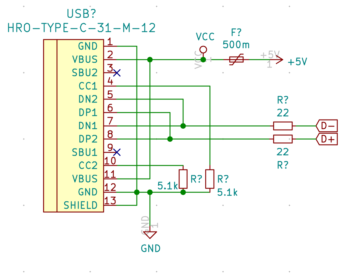
Reset Circuit

The USB connector

USB Type-C connector are much more usable than Type-B, because they can be reversed. The USB circuit needs to be as protective as possible for the rest of the keyboard electronics as I don’t want the electronic components to be destroyed by an electrostatic discharge (ESD). This means the circuit will have ESD protection on the data lines and power surge protection on the Vcc.

But for ease of building, the USB-C connector must be hand solderable. I had a good experience with the HRO Type-C-31-M-12. It is reasonably cheap, available and easy to hand-solder. Though, the shield contacts don’t completely go through a standard 1.6mm PCB (which is not an issue with metalized holes or thinner PCBs). It’s an USB 2.0 Type-C connector, perfect for a keyboard that doesn’t require hi-speed transfer.

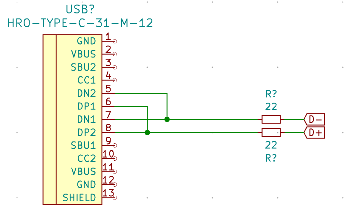
So, let’s add a HRO-TYPE-C-31-M12 component to the schema. It is part of ai03’s Type-C library. An USB-C connector has 2x2 USB 2.0 signal wires, two D+ (DP1 and DP2) and two for D- (respectively DN1 and DN2). The reason there are 2 sets of lines is to provide the reversibility of the connector. We’ll start by connecting those together, with 22 ohms resistors as the Atmega32U4 data-sheet requires:

USB-C DN/DP signals

Next, wire both GND and the shield together, then both VBUS pins:

USB-C VBUS/GND

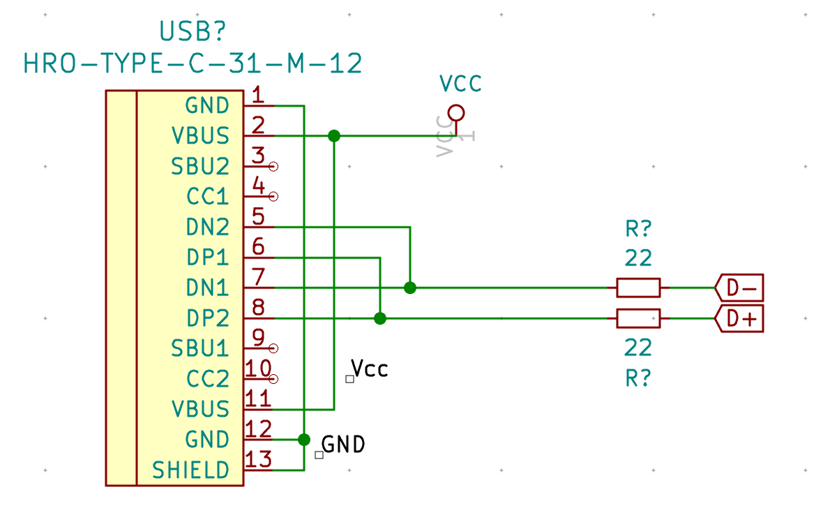
Note that we haven’t declared the +5V signal we’ve used elsewhere in the schema, instead we’ve declared Vcc. We’re going to add a fuse in the next step to protect our +5V against current surge.

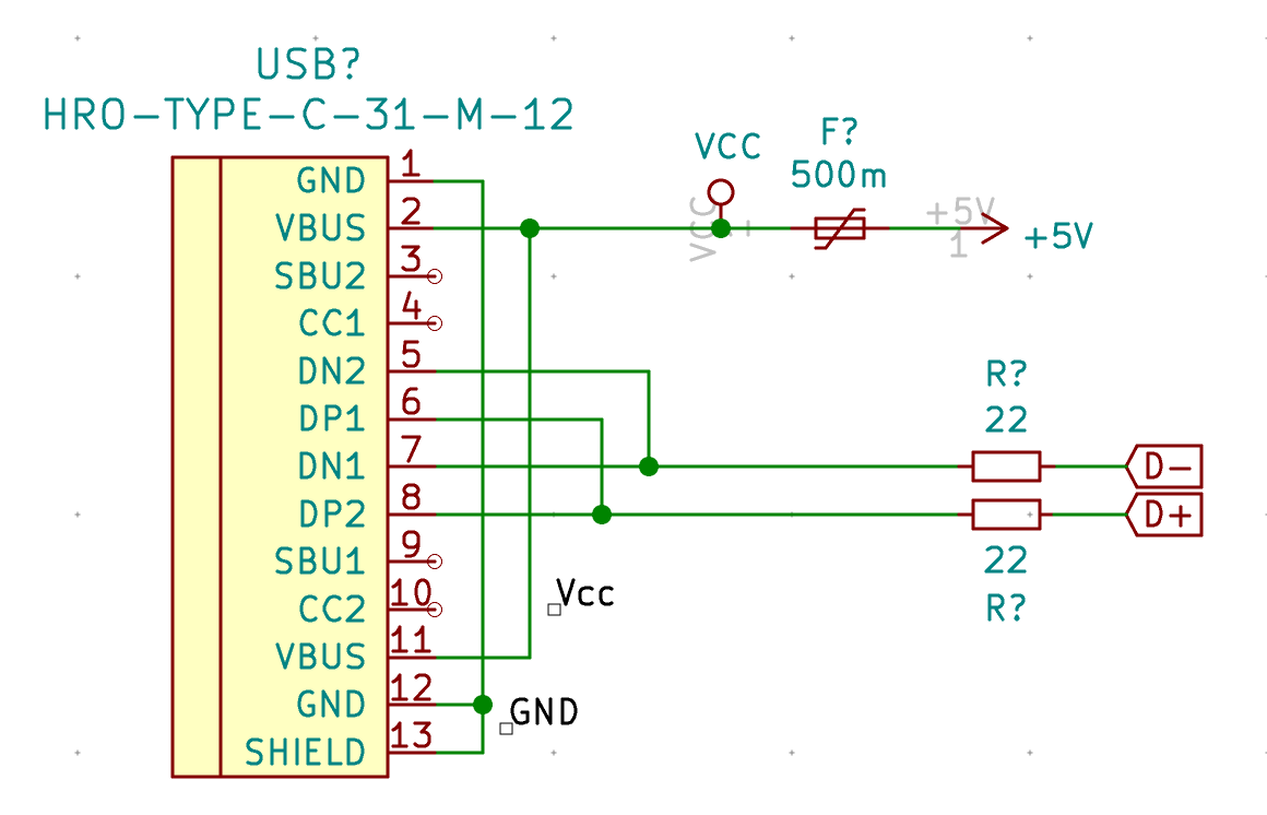
Add a Polyfuse_Small to the schema connected to Vcc and +5V likes this:

USB-C VBUS/GND

SBU1 and SBU2 are not used (it’s only for Alternate Mode like transporting HDMI or thunberbolt signals), so we can use the ‘No connect flag’ (Shift-Q) to place a black cross on those pins.

Next let’s focus a bit on the CC1 and CC2 pins. Those pins are the Channel Configuration pins. They are used to detect cable attachment and removal detection, plug orientation detection, etc.

The mechanism can be modeled like this:

USB-C CC1 in use

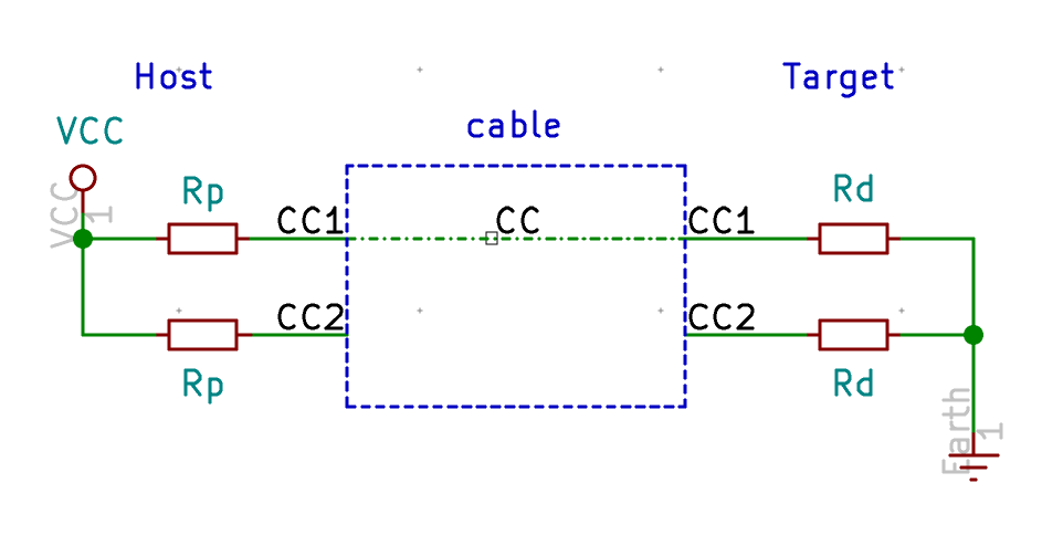
In the above schema we have the host (on the left) connected to the target (our keyboard on the right). Both equipments have pull-up (Rp) or pull-down (Rd) resistors. The USB-C cable has only one connector for CC. In the example above, the host will pull up the level of its CC1 and CC2 pins thanks to the pull-up resistor. The cable connects CC1 on the host to CC1 on the target, creating a current path from the +5V to GND. The host CC1 pin will then have a voltage of less than 5V, while CC2 will still has 5V (no charge). The host then knows the cable is connected (otherwise there would be 5V on both CC1 and CC2) and to which side it is connected to, magic!

Now if we flip the connector at the host for instance, we get the following schema:

USB-C CC2 in use

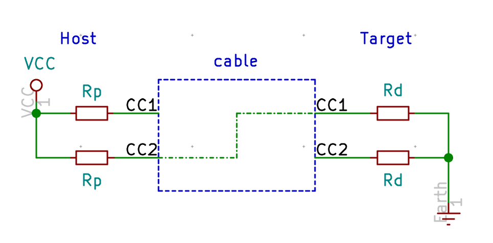
CC2 on the host will see less than 5V but CC1 will see 5V. The host detects it is connected through CC2 and not CC1 as in the previous example.

But there’s more. By choosing properly the value of the Rd resistors we can tell the host, as a target how much current we need to operate. For the USB standard 500mA (which is enough for powering our keyboard), we need 5.1k ohms resistors.

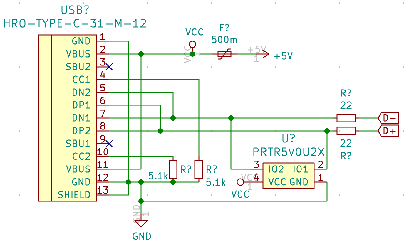
Let’s modify our schema now to add the CC pull-down resistors:

USB-C CC Pull Down

And finally we’re going to add the ESD protection system. We could use rail to rail discrete diodes, but it’s way easier to use an IC. There are several possibilities, one of the simplest is the PRTR5V0U2X. But you might find also the USBLC6 on some designs.

Here’s the modified schema with the PRTR5V0U2X connected to the data lines:
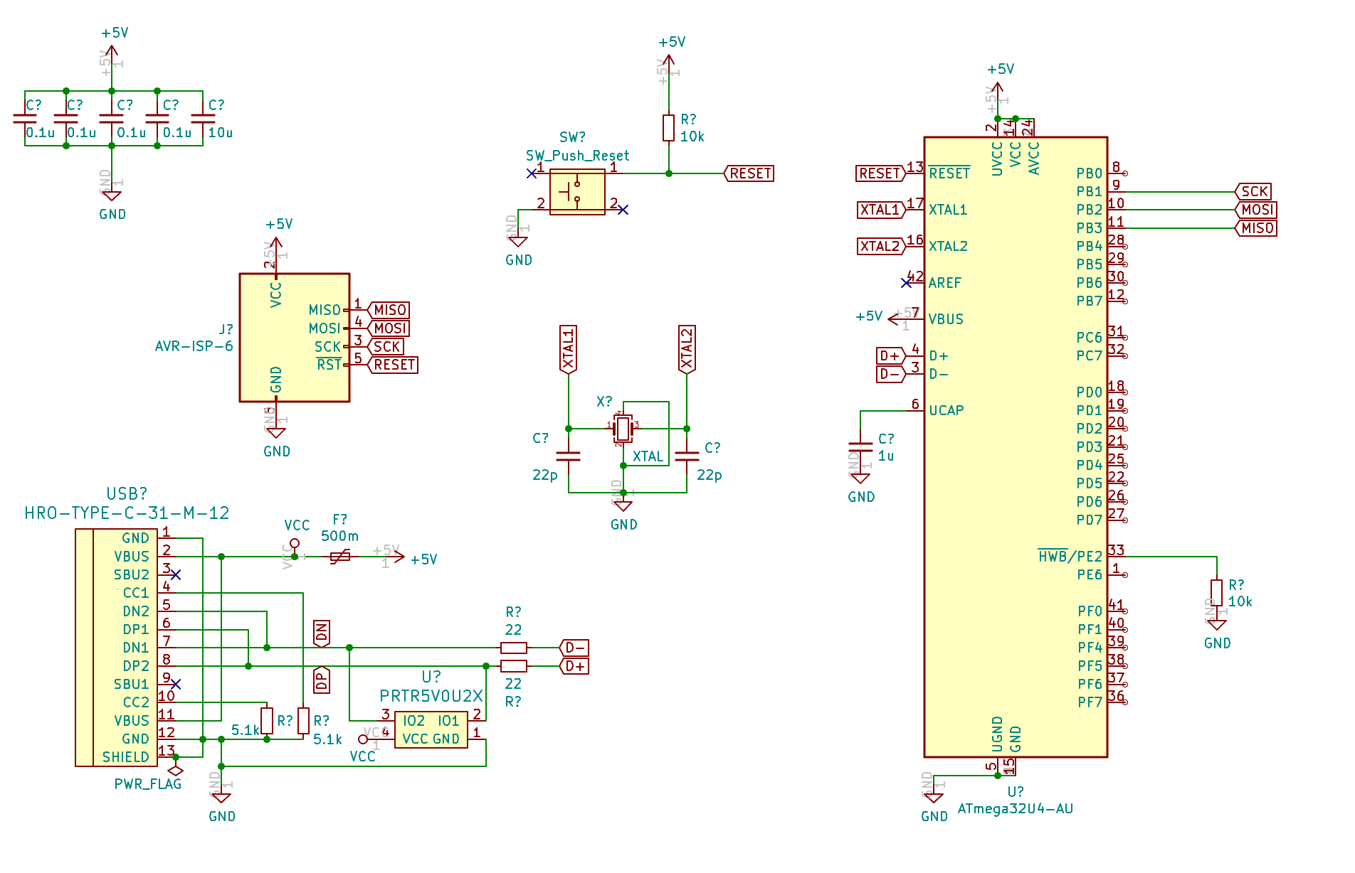
USB-C with the PRTR5V0U2X

The big picture

If you followed the design so far, you should have the following schema:

The big picture

What’s cooking next

We’re far from having a working PCB. I’m going to cover the following topics in the next episode:

  • design the matrix
  • reference the components
  • check the EDC rules
  • starts laying out the PCB

Then on the subsequent parts, I’ll cover soldering SMD components, configuring the firmware, testing the PCB, and designing the case.

Want to read the next part? Then click here for the Designing a Keyboard part 2

Handwired Keyboard Build Log - Part 2

17 minute read

In the handwired build log part 1 we saw a technique to build a nice keyboard matrix without using a PCB.

In this part we’ll discover how to hook the teensy controller to the matrix.

The needed tools & parts

For this part, we’ll use:

  • the soldering station and solder
  • a pair of tweezers
  • a sharp knife
  • a wrench
  • a philips screwdriver

We’ll also need those parts:

Preamble

We plan to put the controller on a ribbon cable DIP connector:

the ribbon cable DIP connector

This is a special connector normally used to solder a ribbon cable to a PCB. This connector has the same footprint as a teensy, so instead of soldering it to a PCB, we’ll solder the teensy on the connector.

The ribbon cable will go from this connector to the matrix. To secure the ribbon cable, we need to use some wrench to crimp the connector on the ribbon cable. Each conductor from the ribbon cable ends up on a pin of the DIP connector:

the ribbon cable and the teensy

For the controller to read the matrix we need to wire each row and each column to a given port on the MCU. The good thing is that any port will do it, we don’t need to wire specifically a column or a row to a specific port (this would have been different if we had backlight leds which work better with a PWM capable pin).

An upcoming case?

I didn’t plan any case, but I want in the end to put a transparent PMMA bottom on which I could glue the controller. Since the plate has 5 M2 screw holes, I plan to secure the bottom plate through these holes by using the screws and five PCB brass spacers.

Wiring the matrix to the controller

We have 12 columns and 4 rows in the matrix, all those needs to be connected to the MCU ports. That means we’re going to use 16 conductors out of 24 on our ribbon cable.

For aesthetic reasons, and since 12 is a multiple of 4, I’ve splitted the 16 conductors ribbon cable in 4 pieces of 4 conductors.

The idea is to route the 4 conductors ribbon up to where the individual connector will be soldered to the matrix.

The big difficulty is to plan the length of the 4 conductors ribbons and when to split them in individual conductors. Again for aesthetic reasons, I decided to keep the conductors bound together in the ribbon as much as physically possible.

The other good news is that a small ribbon of 4 conductors is about the same size as the distnce between 2 switches. So I can route those ribbons easily under the matrix wires and between the switches up to their respective destinations.

For aesthetic reason again, I decided to route all the ribbons starting from the controller at the same place in the back of the board, and make some 90º turns when needed. So I need to route them sorted by length (ie start by routing the longest ribbon and finish by the smallest one).

routing 2 first 4 conductors ribbons

As you can see in the picture, the ribbons turn around the brass spacers. I started routing from the middle lane which was free of spacers until the middle of the plate, then move up or down to access the needed columns.

One thing I didn’t plan very well was that I wanted the controller and its USB port to be on the left of the keyboard. But I did the routing from the left when the keyboard was on the front, so in the end the controller happens to be on the right side. Unfortunately it was to late to change it when I noticed it.

To connect the conductors to the matrix columns, I splitted the ribbon in individual connectors and routed them each to one switch:

end of a ribbon

Then it is a matter of cutting the conductor to the right length and remove the insulator. Usually it is not possible to use the wire stripper because it requires a large distance between the cut position and the end of the cable which is not possible when the conductor comes from the plate. I had to remove the insulator using a sharp knife and my nails.

To solder the conductors on the columns, I did a loop with the copper conductors around an existing solder junction, then used the solder iron to heat that existing solder. The loop was incorporated into the existing junction solder easily:

soldering individual conductors

Since we have 12 columns, I decided to route the first 4 conductors ribbon to the column 1 to 4 (the right ones on the back), the second ribbon to the middle ones (5 to 8), and the last column ribbons on the 8 to 12 columns. To balance a bit the routing, the first ribbons connect to the bottom row, the second one to the top row:

wiring all columns

The very next step is to route the last 4 conductors ribbon to the rows. The simples solution was to split the 4 conductors ribbon into 2 parts, one going up and one going down. Then solder the wires to the rows on the same column.

routing to the rows

And the final routing result:

routing final results

Soldering the controller

The first step is to crimple the DIP support on the ribbon cable. To help aligning the 16 conductors ribbon, I kept the unused 8 conductors part (this way the ribbon can’t move while closing the support).

the DIP support

To prevent any electric short between the controller and the switches, the controller is placed upside down, so the support pins are facing down in usual conditions (so the pins are facing up when the keyboard is reversed as in the picture).

Before soldering the controller to the support, I used the multimeter to make sure all the support pins are correctly connected to the matrix. To do that place the black electrode of the multimeter to one of the pin and check it is connected to the correct column or row.

At the same time note which pin is connected to which column or row, as we’ll have to use this information for the firmware:

the Teensy pins/port

If you follow exactly this tutorial, you’ll end up with this table for the rows:

row pin port
1 23 C6
2 11 D7
3 24 D7
4 12 D6

And this one for the columns:

Column pin port
1 19 D0
2 7 F7
3 20 D1
4 8 B6
5 22 D3
6 9 B5
7 21 D2
8 10 B4
9 9 F6
10 18 B7
11 17 B3
12 6 F5

Then solder the Teensy controller. It’s not easy as the Teensy PCB pads are very small, so better use a magnifying glass and a very small solder diameter (0.6mm for instance).

Teensy soldered

Programming the controller

To program the controller we’ll use QMK. This is an open source keyboard firmware forked and enhanced from TMK. It supports a miriad of custom keyboards and MCU (including various ATmega and ARM micro-controllers).

First, let’s clone the project:

git clone git@github.com:qmk/qmk_firmware.git
cd qmk_firmware

Then install the ATmega toolchain to be able to build the firmware for our keyboard. It’s very easy with the install process:

./util/qmk_install.sh

On macos it requires Homebrew.

Once done, check that you can compile a firmware, for instance the default GH60 keymap (a very well known 60% PCB):

% make gh60:default
QMK Firmware 0.6.193
Making gh60 with keymap default

avr-gcc (GCC) 7.3.0
Copyright (C) 2017 Free Software Foundation, Inc.
This is free software; see the source for copying conditions.  There is NO
warranty; not even for MERCHANTABILITY or FITNESS FOR A PARTICULAR PURPOSE.

Compiling: keyboards/gh60/gh60.c                                                                    [OK]
Compiling: keyboards/gh60/keymaps/default/keymap.c                                                  [OK]
Compiling: quantum/quantum.c                                                                        [OK]
Compiling: quantum/keymap_common.c                                                                  [OK]
Compiling: quantum/keycode_config.c                                                                 [OK]
Compiling: quantum/matrix.c                                                                         [OK]
...
Compiling: lib/lufa/LUFA/Drivers/USB/Core/USBTask.c                                                 [OK]
Linking: .build/gh60_default.elf                                                                    [OK]
Creating load file for flashing: .build/gh60_default.hex                                            [OK]
Copying gh60_default.hex to qmk_firmware folder                                                     [OK]
Checking file size of gh60_default.hex                                                              [OK]
 * The firmware size is fine - 16926/28672 (11746 bytes free)

You should obtain the gh60_default.hex file. You can remove it, we won’t use it.

QMK supports many keyboards and many layouts (called keymaps in QMK) for each keyboard. A keyboard is defined by a directory in the keyboards/ folder, and each keymap is also a directory in the keymaps/ folder of a keyboard. To build such keymap, one need to use the make <keyboard>:<keymap> command.

The make command produces a hex file that can be flashed on the controller with QMK Toolbox, which is the recommended method. We can flash from the command line if we know the controller bootloader type, but QMK Toolbox is able to autodetect the correct bootloader, check the file size and so on. QMK Toolbox also acts as a console for the controller allowing to see debug statements.

For the Teensy, we’ll use the “halfkay” bootloader. One advantage of the Teensy compared to the Pro Micro controller (which we could have used), is that the bootloader is very forgiving: for instance a Pro Micro can be bricked if we flash a firmware that is too large for it.

Let’s implement our own Planck layout. The very first step is to create a new kind of keyboard in the handwired/ keyboard folder. Since it is a Planck keyboard, let’s create a planck folder in which we need to add the following files:

  • a keymaps/ folder (in which we’ll create our own default keymap)
  • a rules.mk makefile which contains our keyboard definition and QMK features enabled
  • a config.h which defines how our matrix is connected to the controller ports
  • a planck.c and planck.h which only defines the keymap macro in our case

You can find all the files in my QMK Handwired Planck branch.

Here’s a condensed version of my config.h:

/* key matrix size */
#define MATRIX_ROWS 4
#define MATRIX_COLS 12

/* Our handwired pin-out */
#define MATRIX_ROW_PINS { C6, D7, C7, D6 }
#define MATRIX_COL_PINS { D0, F7, D1, B6, D3, B5, D2, B4, F6, B7, B3, F5 }
#define UNUSED_PINS { B0, B1, B2, F0, F1, F4, D4, D5, E6 }

/* COL2ROW or ROW2COL */
#define DIODE_DIRECTION COL2ROW

We defined here that the matrix is 4x12, and the ports of the rows and columns (in increasing order). Also, we tell QMK that we hooked the diodes between the columns and the rows.

In rules.mk, we tell QMK everything about the used controller:

# This is a teensy 2.0
BOOTLOADER = halfkay
# running this MCU
MCU = atmega32u4
# Processor frequency.
F_CPU = 16000000
# Target architecture (see library "Board Types" documentation).
ARCH = AVR8
# Input clock frequency.
F_USB = $(F_CPU)
# Interrupt driven control endpoint task(+60)
OPT_DEFS += -DINTERRUPT_CONTROL_ENDPOINT
# Boot Section Size in *bytes*
#   Teensy halfKay   512
OPT_DEFS += -DBOOTLOADER_SIZE=512
# Build Options
BOOTMAGIC_ENABLE = no       # Virtual DIP switch configuration(+1000)
MOUSEKEY_ENABLE = no        # Mouse keys(+4700)
EXTRAKEY_ENABLE = yes       # Audio control and System control(+450)
CONSOLE_ENABLE = yes        # Console for debug(+400)
COMMAND_ENABLE = yes        # Commands for debug and configuration
NKRO_ENABLE = no            # Nkey Rollover
BACKLIGHT_ENABLE = no       # There are no leds
MIDI_ENABLE = no            # No MIDI controls
AUDIO_ENABLE = no           # We don't have audio
UNICODE_ENABLE = no         # Unicode
BLUETOOTH_ENABLE = no       # We don't have BT
RGBLIGHT_ENABLE = no        # We don't have underglow

I then created the default keymap. Since this is a Planck replica, I copied over the default Planck keymap of the MIT (2u space) layout. A keymap is a folder in the keymaps/ folder.

Usually the layout is described in the keymap.c file.

This keymap is a 3 layers keymap (base, raise, lower). The base layer can be either qwerty (the default), colemak or dvorak.

A layer is a 2D array representing the keycode associated with a matrix switch. A keymap is an array of layouts (see the keymaps symbol in the keymap.c), one per layer.

The keyboard can be in only one layer at a time, and can be programmed to switch to a given layer with a key combination as explained below.

Here’s for example the keymap of the base qwerty layer of my Planck handwired keyboard:

const uint16_t PROGMEM keymaps[][MATRIX_ROWS][MATRIX_COLS] = {
/* Qwerty
 * ,-----------------------------------------------------------------------------------.
 * | Tab  |   Q  |   W  |   E  |   R  |   T  |   Y  |   U  |   I  |   O  |   P  | Bksp |
 * |------+------+------+------+------+-------------+------+------+------+------+------|
 * | Esc  |   A  |   S  |   D  |   F  |   G  |   H  |   J  |   K  |   L  |   ;  |  '   |
 * |------+------+------+------+------+------|------+------+------+------+------+------|
 * | Shift|   Z  |   X  |   C  |   V  |   B  |   N  |   M  |   ,  |   .  |   /  |Enter |
 * |------+------+------+------+------+------+------+------+------+------+------+------|
 * | Brite| Ctrl | Alt  | GUI  |Lower |    Space    |Raise | Left | Down |  Up  |Right |
 * `-----------------------------------------------------------------------------------'
 */
[_QWERTY] = LAYOUT_planck_grid(
    KC_TAB,  KC_Q,    KC_W,    KC_E,    KC_R,    KC_T,    KC_Y,    KC_U,    KC_I,    KC_O,    KC_P,    KC_BSPC,
    KC_ESC,  KC_A,    KC_S,    KC_D,    KC_F,    KC_G,    KC_H,    KC_J,    KC_K,    KC_L,    KC_SCLN, KC_QUOT,
    KC_LSFT, KC_Z,    KC_X,    KC_C,    KC_V,    KC_B,    KC_N,    KC_M,    KC_COMM, KC_DOT,  KC_SLSH, KC_ENT ,
    BACKLIT, KC_LCTL, KC_LALT, KC_LGUI, LOWER,   KC_SPC,  KC_SPC,  RAISE,   KC_LEFT, KC_DOWN, KC_UP,   KC_RGHT
),
...
}

This corresponds to this layout:

Planck qwerty layout

All the people I showed the keyboard asked my why the Esc key is placed below the Tab key. I’m assuming that the original Planck layout has been built this way to enhance the VIM experience. This way the Esc key is on the homerow and can be reached without moving the left hand.

The LAYOUT_planck_grid macro has been defined in our planck.h file. It just maps a keycode to a spot in the layer array representing the matrix.

Notice the two RAISE and LOWER special keycodes. They are layer keycodes defined like this:

#define LOWER MO(_LOWER)
#define RAISE MO(_RAISE)

The MO(layer) macro allows to temporarily activate the given layer when the key is pressed.

The _LOWER and _RAISE layers are defined like this:

...
/* Lower
 * ,-----------------------------------------------------------------------------------.
 * |   ~  |   !  |   @  |   #  |   $  |   %  |   ^  |   &  |   *  |   (  |   )  | Bksp |
 * |------+------+------+------+------+-------------+------+------+------+------+------|
 * | Del  |  F1  |  F2  |  F3  |  F4  |  F5  |  F6  |   _  |   +  |   {  |   }  |  |   |
 * |------+------+------+------+------+------|------+------+------+------+------+------|
 * |      |  F7  |  F8  |  F9  |  F10 |  F11 |  F12 |ISO ~ |ISO | | Home | End  |      |
 * |------+------+------+------+------+------+------+------+------+------+------+------|
 * |      |      |      |      |      |             |      | Next | Vol- | Vol+ | Play |
 * `-----------------------------------------------------------------------------------'
 */
[_LOWER] = LAYOUT_planck_grid(
    KC_TILD, KC_EXLM, KC_AT,   KC_HASH, KC_DLR,  KC_PERC, KC_CIRC, KC_AMPR,    KC_ASTR,    KC_LPRN, KC_RPRN, KC_BSPC,
    KC_DEL,  KC_F1,   KC_F2,   KC_F3,   KC_F4,   KC_F5,   KC_F6,   KC_UNDS,    KC_PLUS,    KC_LCBR, KC_RCBR, KC_PIPE,
    _______, KC_F7,   KC_F8,   KC_F9,   KC_F10,  KC_F11,  KC_F12,  S(KC_NUHS), S(KC_NUBS), KC_HOME, KC_END,  _______,
    _______, _______, _______, _______, _______, _______, _______, _______,    KC_MNXT,    KC_VOLD, KC_VOLU, KC_MPLY
),

/* Raise
 * ,-----------------------------------------------------------------------------------.
 * |   `  |   1  |   2  |   3  |   4  |   5  |   6  |   7  |   8  |   9  |   0  | Bksp |
 * |------+------+------+------+------+-------------+------+------+------+------+------|
 * | Del  |  F1  |  F2  |  F3  |  F4  |  F5  |  F6  |   -  |   =  |   [  |   ]  |  \   |
 * |------+------+------+------+------+------|------+------+------+------+------+------|
 * |      |  F7  |  F8  |  F9  |  F10 |  F11 |  F12 |ISO # |ISO / |Pg Up |Pg Dn |      |
 * |------+------+------+------+------+------+------+------+------+------+------+------|
 * |      |      |      |      |      |             |      | Next | Vol- | Vol+ | Play |
 * `-----------------------------------------------------------------------------------'
 */
[_RAISE] = LAYOUT_planck_grid(
    KC_GRV,  KC_1,    KC_2,    KC_3,    KC_4,    KC_5,    KC_6,    KC_7,    KC_8,    KC_9,    KC_0,    KC_BSPC,
    KC_DEL,  KC_F1,   KC_F2,   KC_F3,   KC_F4,   KC_F5,   KC_F6,   KC_MINS, KC_EQL,  KC_LBRC, KC_RBRC, KC_BSLS,
    _______, KC_F7,   KC_F8,   KC_F9,   KC_F10,  KC_F11,  KC_F12,  KC_NUHS, KC_NUBS, KC_PGUP, KC_PGDN, _______,
    _______, _______, _______, _______, _______, _______, _______, _______, KC_MNXT, KC_VOLD, KC_VOLU, KC_MPLY
),
...

Since on a 40% keyboard we can’t have access to the numbers, function keys, and most of the symbols, those are placed on a different layer than the regular direct access keys. The two raise/lower keys can be actionned by the left and right thumb while at the same time pressing another key to obtain the number or symbol. This is very efficient.

The _______ is an alias for KC_TRANS which means that this key isn’t defined in this layer. When pressing this key while being in this layer, the keycode that will be emited is the first one to not be KC_TRANS in the layer stack. That means that Enter for instance is still Enter in any of the RAISE or LOWER layer.

The rest of the keymap.c file contain special code that overrides the default QMK behavior.

In QMK, a keyboard can override some functionalities, and a keymap can override the keyboard override.

For instance we overrode the process_record function by defining the process_record_user function in our keymap. This is a function which is called each time a key event happens (a key pressed or released). In our case, this is used to switch to a different base layer when going to the ADJUST layer and pressing a base layer key (for instance it is K to switch to colemak). The ADJUST layer is obtained by pressing at the same time the LOWER and RAISE keys.

We also overrode layer_state_set_user to make the LOWER + RAISE = ADJUST layer switching work. The layer_state_set_user function is called whenever QMK is switching to another layer, giving a chance to modify the target layer. We used update_tri_layer_state to return ADJUST when we switched to both LOWER and RAISE.

Now let’s build our firmware:

% make handwired/planck:default
QMK Firmware 0.6.193
Making handwired/planck with keymap default

avr-gcc (GCC) 7.3.0
Copyright (C) 2017 Free Software Foundation, Inc.
This is free software; see the source for copying conditions.  There is NO
warranty; not even for MERCHANTABILITY or FITNESS FOR A PARTICULAR PURPOSE.

Compiling: keyboards/handwired/planck/planck.c                                                      [OK]
Compiling: keyboards/handwired/planck/keymaps/default/keymap.c                                      [OK]
Compiling: quantum/quantum.c                                                                        [OK]
Compiling: quantum/keymap_common.c                                                                  [OK]
Compiling: quantum/keycode_config.c                                                                 [OK]
Compiling: quantum/matrix.c                                                                         [OK]
Compiling: tmk_core/common/host.c                                                                   [OK]
Compiling: tmk_core/common/keyboard.c                                                               [OK]
Compiling: tmk_core/common/action.c                                                                 [OK]
Compiling: tmk_core/common/action_tapping.c                                                         [OK]
Compiling: tmk_core/common/action_macro.c                                                           [OK]
Compiling: tmk_core/common/action_layer.c                                                           [OK]
Compiling: tmk_core/common/action_util.c                                                            [OK]
Compiling: tmk_core/common/print.c                                                                  [OK]
Compiling: tmk_core/common/debug.c                                                                  [OK]
Compiling: tmk_core/common/util.c                                                                   [OK]
Compiling: tmk_core/common/eeconfig.c                                                               [OK]
Compiling: tmk_core/common/report.c                                                                 [OK]
Compiling: tmk_core/common/avr/suspend.c                                                            [OK]
Compiling: tmk_core/common/avr/timer.c                                                              [OK]
Compiling: tmk_core/common/avr/bootloader.c                                                         [OK]
Assembling: tmk_core/common/avr/xprintf.S                                                           [OK]
Compiling: tmk_core/common/magic.c                                                                  [OK]
Compiling: tmk_core/common/command.c                                                                [OK]
Compiling: tmk_core/protocol/lufa/lufa.c                                                            [OK]
Compiling: tmk_core/protocol/usb_descriptor.c                                                       [OK]
Compiling: tmk_core/protocol/lufa/outputselect.c                                                    [OK]
Compiling: lib/lufa/LUFA/Drivers/USB/Class/Common/HIDParser.c                                       [OK]
Compiling: lib/lufa/LUFA/Drivers/USB/Core/AVR8/Device_AVR8.c                                        [OK]
Compiling: lib/lufa/LUFA/Drivers/USB/Core/AVR8/EndpointStream_AVR8.c                                [OK]
Compiling: lib/lufa/LUFA/Drivers/USB/Core/AVR8/Endpoint_AVR8.c                                      [OK]
Compiling: lib/lufa/LUFA/Drivers/USB/Core/AVR8/Host_AVR8.c                                          [OK]
Compiling: lib/lufa/LUFA/Drivers/USB/Core/AVR8/PipeStream_AVR8.c                                    [OK]
Compiling: lib/lufa/LUFA/Drivers/USB/Core/AVR8/Pipe_AVR8.c                                          [OK]
Compiling: lib/lufa/LUFA/Drivers/USB/Core/AVR8/USBController_AVR8.c                                 [OK]
Compiling: lib/lufa/LUFA/Drivers/USB/Core/AVR8/USBInterrupt_AVR8.c                                  [OK]
Compiling: lib/lufa/LUFA/Drivers/USB/Core/ConfigDescriptors.c                                       [OK]
Compiling: lib/lufa/LUFA/Drivers/USB/Core/DeviceStandardReq.c                                       [OK]
Compiling: lib/lufa/LUFA/Drivers/USB/Core/Events.c                                                  [OK]
Compiling: lib/lufa/LUFA/Drivers/USB/Core/HostStandardReq.c                                         [OK]
Compiling: lib/lufa/LUFA/Drivers/USB/Core/USBTask.c                                                 [OK]
Linking: .build/handwired_planck_default.elf                                                        [OK]
Creating load file for flashing: .build/handwired_planck_default.hex                                [OK]
Copying handwired_planck_default.hex to qmk_firmware folder                                         [OK]
Checking file size of handwired_planck_default.hex                                                  [OK]
 * The firmware size is fine - 17618/32256 (14638 bytes free)

Our firmware is in the handwired_planck_default.hex file.

To flash it:

  1. Connect the Teensy to the computer
  2. Open QMK Toolbox
  3. Press the Teensy reset button
  4. QMK Toolbox will notice a Teensy is connected by displaying *** Halfkay device connected
  5. Load the firmware
  6. Choose the ATMega32U4 microcontroller
  7. Press the flash button

You should see something like this:

*** Halfkay device connected
*** Attempting to flash, please don't remove device
>>> teensy_loader_cli -mmcu=atmega32u4 /Users/brice/devl/qmk_firmware/handwired_planck_default.hex -v
    Teensy Loader, Command Line, Version 2.1
    Read "handwired_planck_default.hex": 17618 bytes, 54.6% usage
    Found HalfKay Bootloader
    Programming..........................................................................................................................................
    Booting
*** Halfkay device disconnected
*** masterzen - Planck connected -- 0xFEED:0x6060

At this point your computer should recognize that a new keyboard has been connected. If you press any switches it should produce a letter.

You can now test the keyboard and the keymap with the Keyboard Tester.

Adding keycaps

It can be hard to find nice 40% ortho keycaps. I used the MDA Big Bang set. It’s a nice, smooth (and not that expensive) thick PBT keyset with dye-sub legends that covers a wide range of ortholinear keyboards, including the Planck.

The MDA (also called MIX or EDRUG) profile is a newer key profile that we could call the little brother of the SA profile. It’s less sculpted than SA, but still more than the other profiles.

Here’s how it looks on this handwired Planck:

My Handwired Planck with MDA Big Bang

What’s coming next

I haven’t had the time to work again on the keyboard, but I want to make it a bit slimmer (it has currently a height of 2cm not including keycaps and switches), and add a transparent bottom plate with small rubber feets.

I plan the bottom plate to be a transparent plexiglass plate (so that we can see the matrix), cut at the size of the metal switch plate. The complex part will be to correctly align the holes for the brass spacer screws along with making sure the hole head fits inside the plate.

To reduce the keyboard height, I will have to carve a small part of the bottom plate so that a small part of the teensy height can fit inside.

If possible, I’d like to build a full case made of plexiglass. I need to design it properly and find the correct tools to do that.

This will probably be the part 3 of this series!

Handwired Keyboard Build Log - Part 1

10 minute read

Update 1: I’ve finished the second part of the serie

Update 2: The plate I’m using has a height of 1.5mm, not 2.5mm as some astute readers have pointed out.

For the last 7 months, I’ve been discovering a new hobby: DIY mechanical keyboards. I’ve been using mechanical keyboards for ages (I was mostly typing on a Code keyboards lately), but lately moved to type only on my macbook keyboard (hopefully this is an early 2015, so the keyboard ie bearable).

So 7 months ago, I was browsing the Internet when I discovered a new world: there were passionate people that are building their keyboards and even programming them with QMK.

I soon was embarked in a no return journey to find the perfect keyboard, made of custom keyboards purchased from Korean Group Buys, properly prepared keyboard switches, custom color keycaps, split backspace layouts…

Forward to a month ago, I discovered that some people were building their own keyboards without any PCB, I then decided to try following the best handwiring guide with one of the smallest existing keyboard.

This serie of posts is the story behind this keyboard:

the end result

What’s a keyboard anyway

A keyboard if the combination of the following elements:

  • a matrix of switches soldered to a PCB
  • a metal or aluminium plate on which the switches are clipsed to
  • a controller that “reads” the matrix and sends keycodes to the USB port
  • keycaps

So in a very fast loop, the controller’s firmware will power on one column of the matrix and “read” the tension back on the matrix rows. If there’s some tension on one row given current on a column, then the controller can deduce which switch has been pressed. The firmware will then send the corresponding keycode based on the layout to the USB port, and continue with the next column and so on infinitely.

But there’s a problem: if one presses more than one key at a time, it is possible for the controller to register ghost keypresses. See the following schema:

Ghosting Matrix

When the controller will power the Col0, and if K00, K01 and K11 are depressed simultaneously, the controller will read current on both Line0 and Line1, because the current will flow from Col0 to K00 pin 1, then pin 2 because the switch is depressed, then to switch K01, then to switch K11, then to Line1. For the controller it is as if all the switches have been pressed, instead of the 3 that were indeed depressed.

To prevent this we add diodes between the switch and the row it is connected to:

Anti Ghosting Matrix

In the same hypothetical scenario as before, the current will be prevented to flow back from K00 to K01 and from Line0 by the D01 diode. Thus when powering Col0, the controller will only see a tension on Line0. And when powering Col1 it will see a tension from Line0 and Line1, thus registering 3 key presses.

Handwiring

Handwiring as its name implies is an electronic technique of building electronic circuits without using a PCB, and instead wiring all components one by one manually with small electric wires. It is often used to perform prototype of electronic boards.

The aim of this build log is to show how to wire a fully working (but small) keyboard.

The BOM

We’re going to build a Planck like keyboard in MIT layout, that is a matrix of 4x12, with a 2u spacebar, accounting for 47 keys. I chose this keyboard and layout because it’s one of the smaller keyboard (a 40%) and it is ortholinear (all switches are aligned) making it easy to wire.

So what will we need to build our keyboard:

  • 47 switches. I had a left-over of Aliaz silent 70g switches
  • a planck plate (which I purchased pre-made by Laserboost). You can get one either from them or Lasergist if you send them the CAD files. You can easily get the CAD files from the KLE layout tool and swillkb. I choose a 1.5mm metal plate to make sure it is sturdy enough to type on it.
  • electric wire of 0.2mm2 (24 AWG) of different colors
  • 47 diodes 1N4148
  • a controller: teensy 2.0. It can be a Pro Micro or even the newer QMK Proton C.
  • around 30cm of 24 way 1.27mm pitch ribbon cable
  • a ribbon DIP connector to attach to the ribbon cable and solder the teensy

The MIT layout Planck plate looks like this:

Planck Plate

Note that this plate has holes for a PCB mount stabilizer for the 2u space bar. I should have taken a version for a plate mount stabilizer, because with a PCB we won’t be able to put a stabilizer under the space bar.

We’ll also need the following tools:

  • a wire stripper. Being in Europe I got myself a nice Stanley one.
  • a set of tweezers
  • a precision wire cutter
  • a multimeter with continuity mode
  • a soldering station (preferrably temperature controlled) and solder
  • a sharp knife or razor (to remove insulators on very small cables)
  • an usb A to usb mini cable for programming the controller

The most important part is the insulator stripper:

Insulator Stripper

You can get a Vise Grip or any other tool like this one. You might need to tune it’s strength (there’s usually a small knob on the tool) so that it doesn’t cut the small wires.

In this part of the story, we’ll only need the wire stripper, some colored wires, the plate, 47 switches, tweezers, a multimeter, the wire cutter, solder and the soldering station.

Placing the switches

The very first step of our handwiring work is to firmly clips the switches on the plate:

switches on plate

switches on plate

I put the switches facing north (the led hole is at the top) so that the higher pins when seen from the back of the plate will be the pin connected to the rows, and the other one will be connected to the columns.

With a 2.5mm plate, the switches should clipse correctly on it. Make sure the plate is using MX switch holes without “top-opening” punches (straight square holes).

Preparing the diodes

We’ll have to solder the diodes on the switch pin connected to a row. Since there’s no circuit copper pads to put the solder on like on a PCB, the best way to solder something on a pin is to form a small wire loop and put solder on it. The solder will “flow” between the pin and the loop and stick firmly.

So our first task is to form a small loop with one of the leg of the diodes. Make sure to do it on the correct leg: the one opposite to the diode black mark:

diode loop

To ease the process and especially if you got your diodes in bands, you can bend them all in one shot on your desk table like this:

bending diodes

Next, remove the diodes from the strip, and using a tweezer block the wire in it and form a loop by turning around the diode leg. With the tweezer you can make sure the loop is flat. Make sure the loop is big enough to be placed on a switch pin, if not open it a little bit with the tweezers.

Repeat this for the other 46 diodes.

After this you can cut the extraneous diode leg just after the loop:

all diodes

Soldering the diodes

The very next step is to place the diode loops on each of the switch row pins:

placing diodes

And then soldering them:

soldering diodes

Make sure to orient correctly the diodes and leave the other leg correctly aligned.

Notice that I started placing and soldering the diodes from the top row (as seen from the back) so that the other rows diodes long legs doesn’t hinder soldering the next row.

two rows of diodes

We’ll then keep adding diodes and soldering them until we’ve covered all switches:

all diodes soldered

It is important to not cut the remaining leg yet. We’ll use it to connect to the row wire as you’ll find in the next step.

Building the rows

To build the rows, we’ll take a long piece of wire (I used black wire). The first thing to do is to remove the insulator at the loose end on something like 5cm with the wire stripper.

We know that we have 12 switches on a row (except the bottom one which has only 11 switches). There is 19mm between two switches.

Instead of cutting 11 pieces of wire which will be hard to solder in place correctly, we’ll use only one long straight piece of wire on which we’ll split the insulator with the wire stripper into 11 pieces of around 16mm each (without cutting the cable). Since it is hard to correctly measure the insulator length while using the wire stripper, I used a visual clue on the wire stripper to approximate the correct length and aligned the insulator pieces with it before cutting.

To solder the wire, we’re going to bend the diode leg around the cable to form a half loop and solder between the insulator pieces. At the same time secure the row wire with the switch central bumps.

We’ll start by soldering the loose end on the first diode, then proceed to the next diode: push the insulator piece toward the first junction, solder and move back the insulator at equal distance:

soldering first diode in a row

For the first diode, I formed a complete loop with the leg around the wire. For the subsequent diode since it is not practical to do that, I’ve done only half loops.

splitting the insulator

Another option which I used at first is to cut the insulator with the wire stripper on each step instead of cutting the 11 pieces at once. So solder one diode leg, cut the insulator at the right lenght, push it toward the last soldered diode, solder the next one, and so on. This is more effective if the distance between switches is variable, otherwise use the first method.

The last diode in the row should also be soldered by forming a full loop with the diode leg around the wire.

It is important to solder the diode leg on the wire before moving to the next diode leg along the row, otherwise the cable could move during the process and nothing would be correctly aligned.

Cut the extraneous wire at both ends and all the remaining legs with the wire cutter and you should obtain something like this:

1st row done

Apply the same technique to the 3 remaining rows. It takes around 10 minutes to solder a 12 switches row:

rows are almost finished

At this stage, you can check with a multimeter that each switch is correctly connected to the wire. Use the multimeter in continuity mode (the multimeter will beep if there is continuity between two junctions), and put the black electrode on one row end and place the red one on every diode junction, there should be a beep. You can also test the continuity of the switches and diodes combination: still with the black electrode on the row, place the red one on the other switch pin and press the switch: the multimeter should beep.

Once you’ve made sure everything works electrically, it is time to move to the columns wiring.

Wiring the columns

For a better visual effect, I’ve decided to wire each column with a different wire color. Unfortunately I couldn’t find 12 different wire colors, so I’ve used only 6 that I repeated twice. I arranged the colors in an approximation of a rainbow.

We’ll use the exact same technique as for the rows, except that we need to split the insulator into only 3 pieces of equal length (there are only 4 rows on this keyboard). To make sure we have enough wire, I didn’t cut it before soldering the last switch in a column.

Since we don’t have the diodes leg to form a loop around the wire, we’ll build loops with the wire around the switch pins:

wire loop around switch leg

Once soldered we can move to the next switch, push back the insulator toward the previous switch, solder the current one and so on:

wire loop around switch leg

Keep doing this until you’ve done all columns. It takes only a few minute per columns once we get the habit.

Since there are only 11 switches on the bottom row, one of the column will span only 3 switches.

The result should look like this:

the matrix is finished

You can then use the multimeter to check the colums are correctly wired, and that no rows is electrically connected to a column.

What’s coming next

In the handwired build log part 2, I’ll explain how to connect the controller to the matrix and how to program the controller to become a working keyboard. We’ll also put some keycaps on.

Another part will explain how I’m going to build a bottom plate for the keyboard.