Designing a keyboard from scratch - Part 2
Updates
- I fixed the passive components footprints to be 0805 instead of 1206, based on a previous design I made. Those are still easy to hand-solder, but leave more empty space around the MCU to route signals.
- The MCU placement and matrix connection schema is now correct. I forgot that it will be under the PCB and thus everything is mirrored.
- Thanks to Druz who discovered there was a mismatch between the reset button in the electronic schema and the footprint
Preamble
Welcome for the second episode of this series of post about designing a full fledged keyboard from scratch. The first episode focused on the electronic schema of the keyboard controller. This episode will cover the following topics:
- how to design the matrix electronic schema
- how to assign references and values to its components
- the first steps of the PCB layout
The matrix
Trust me, it will be probably the most boring part of this series. I’m going to design the electronic schema of 67 switches and diodes.
Since the MCU schema is taking some space in the main sheet, I recommend creating a hierarchical sheet to place the matrix components. This can be done by pressing the s shortcut and clicking anywhere in the schema. The following window should open:
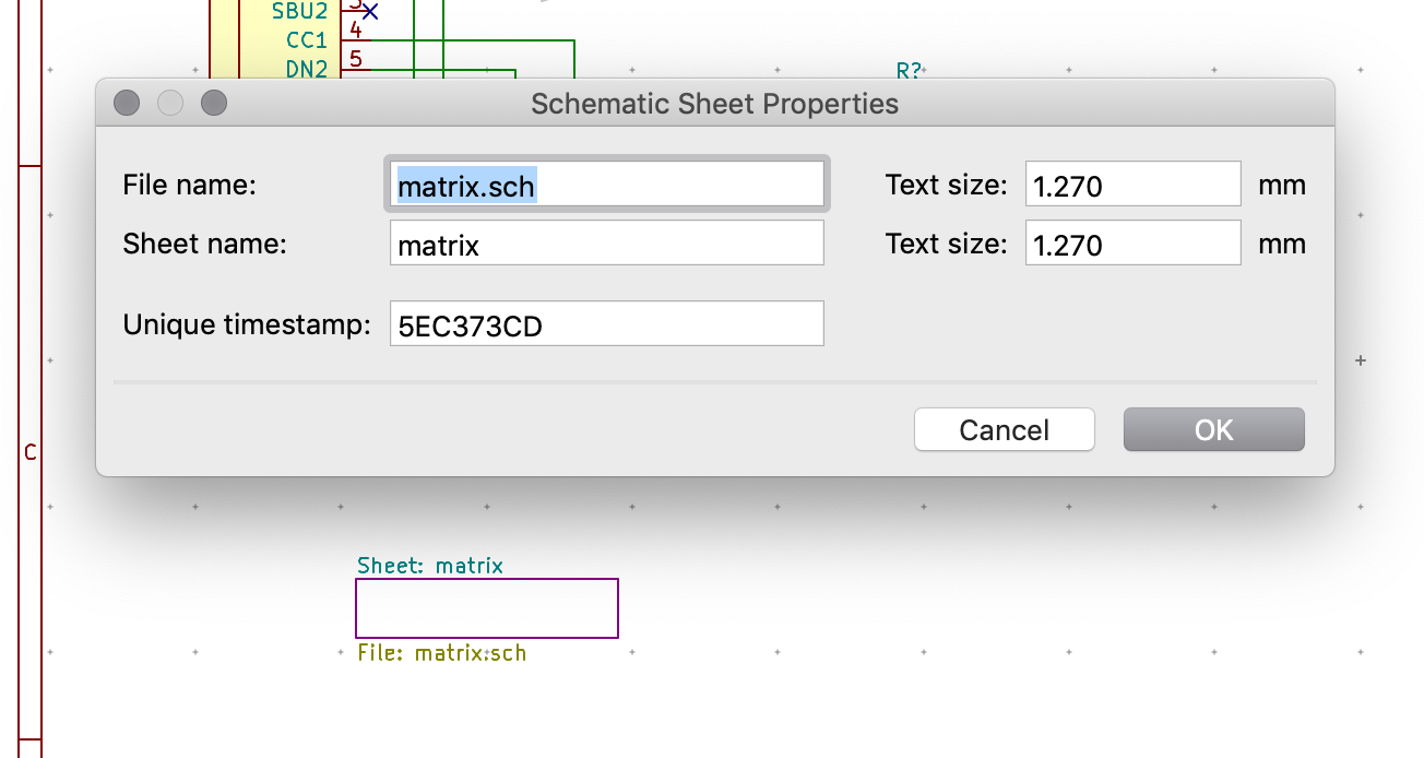
Because I’m designing the matrix, I named this new sheet matrix (yes that’s quite original).
It is possible to access this hierarchical sheet with the View → Show Hierarchical Navigator menu:
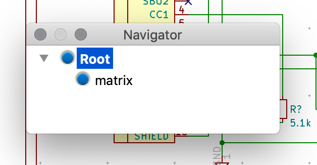
Clicking on the matrix will open this new (blank) schema sheet.
Let’s build the matrix now. As I explained in the previous article, the matrix is the combination of one switch and one diode per key. It’s cumbersome to add those components by hand for all the 67 keys, so I’m going to explain how to do it with a selection copy. There are other ways to do it, for instance by generating the schema with this tool or this other tool.
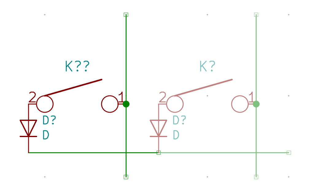
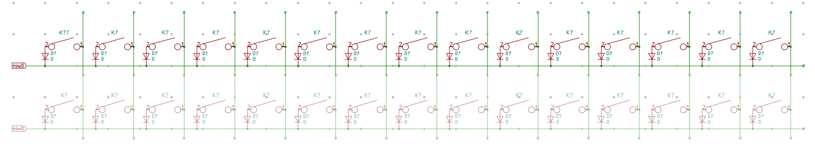
Let’s first design our key cell, by adding a SW_PUSH and a regular D diode. Next wire them as in this schema (notice that there’s no connection between the vertical and horizontal wire):
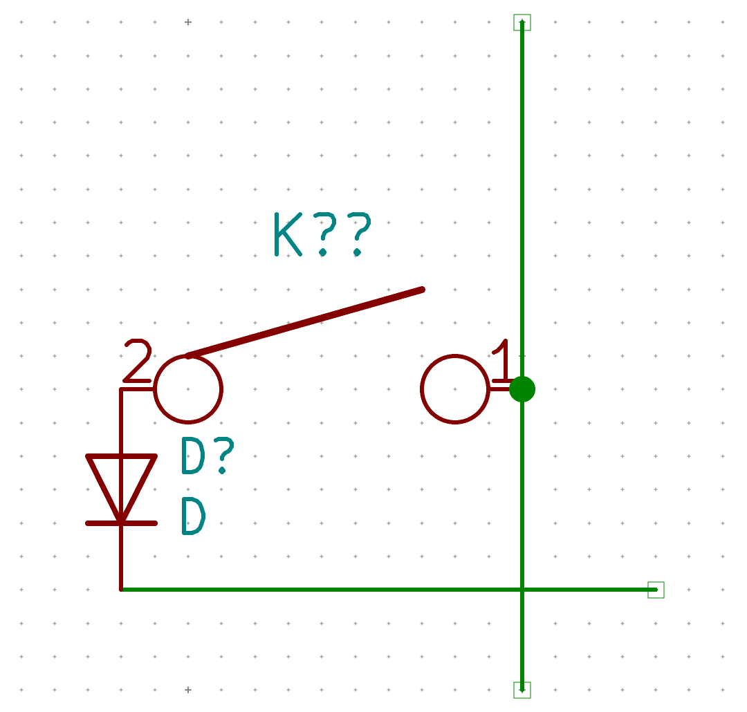
This cell forms the atomic core of the matrix. Once done (if you also are following this for your design make sure the wires have the same size as mine), maintain the shift key depressed and drag a selection around the cell (wire included). This will duplicate the selection (our cell), then move the mouse pointer so that the diode bottom pin is perfectly aligned with the first cell horizontal wire:
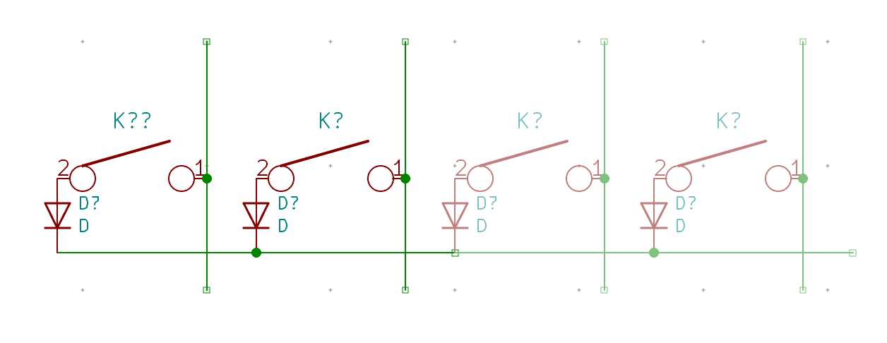
Then click the left mouse button to validate. Now repeat the shift drag selection operation on both cells at once to duplicate them and form a 4 keys schema:
Note that it is also possible to perform the move and place with the keyboard arrow keys and enter to validate.
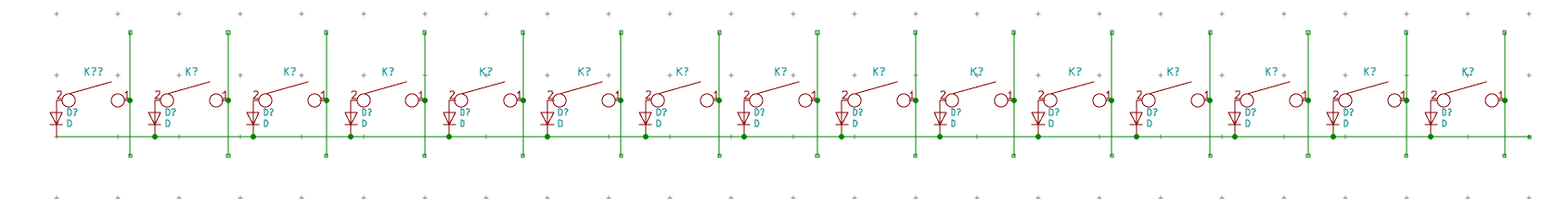
Next, repeat the same with the 4 cells to form a line of 8, then a line of 16 cells, and remove the last one to form a 15 keys row. If the key rows is larger than the page, you can increase the sheet size by going to File → Page Settings and change the Paper Size to A3.
This should look like this:
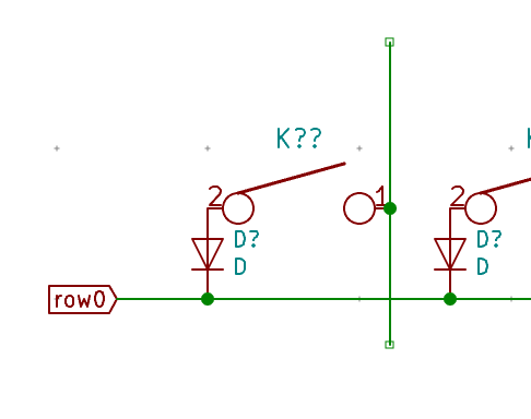
Let’s add a label to the row (Ctrl-H):
Let’s now do the other rows. I’m going to apply the same technique, just do a shift drag selection around the whole row0 and move it downward so that the wires of the columns connect:
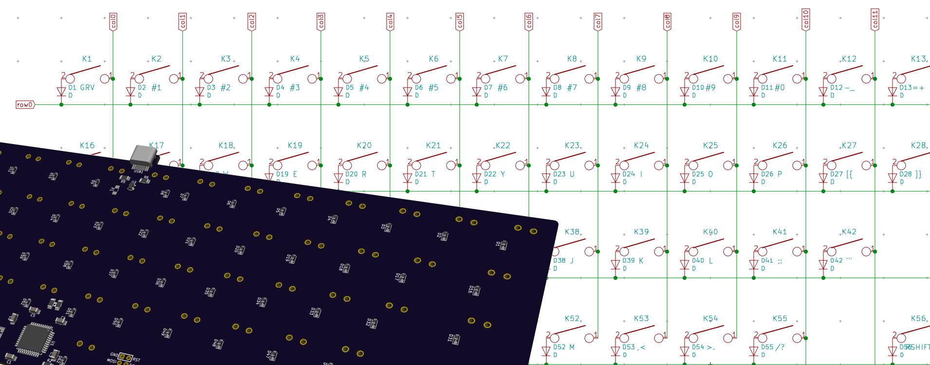
And do the same for the next 3 rows, this will give this nice array of switches:
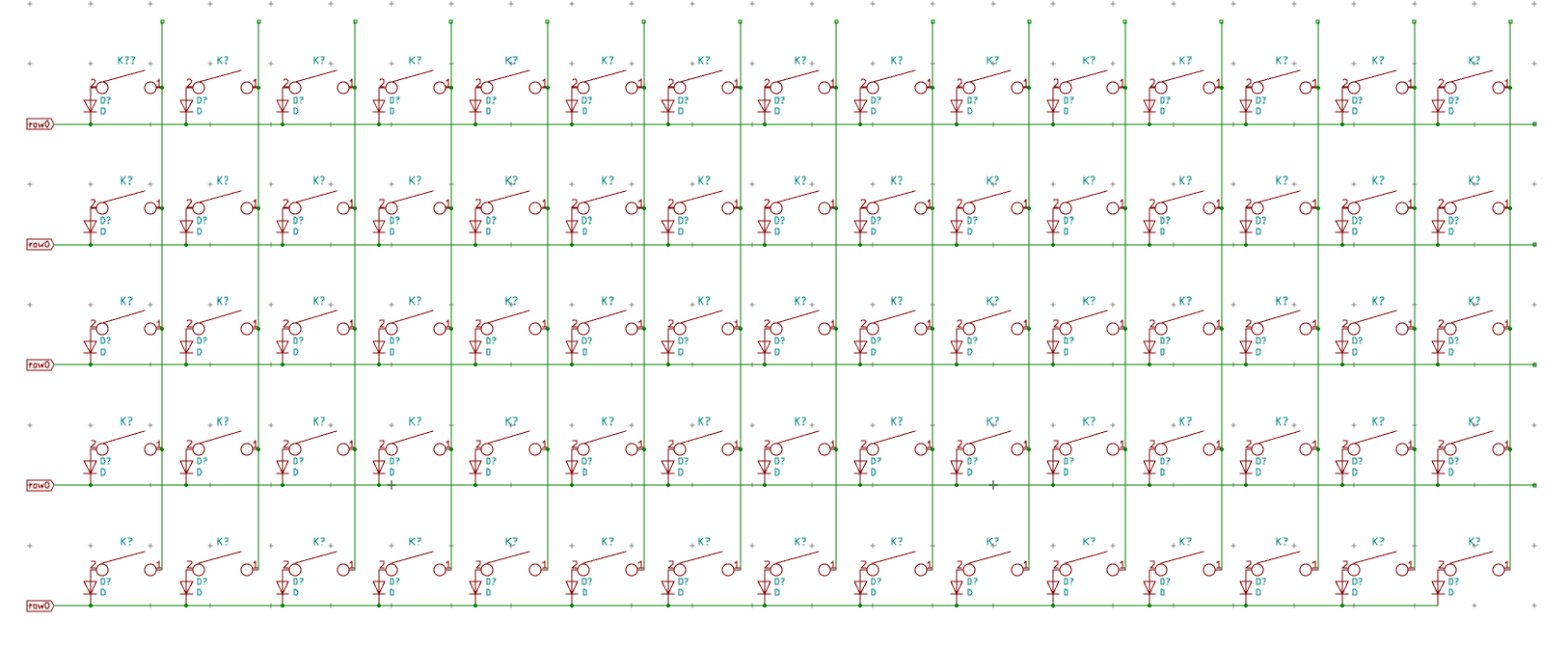
Note that I have pruned the extra vertical wires of the last row with a large regular selection and pressing the del key. It is also possible to do the same for the right extra wires on all rows.
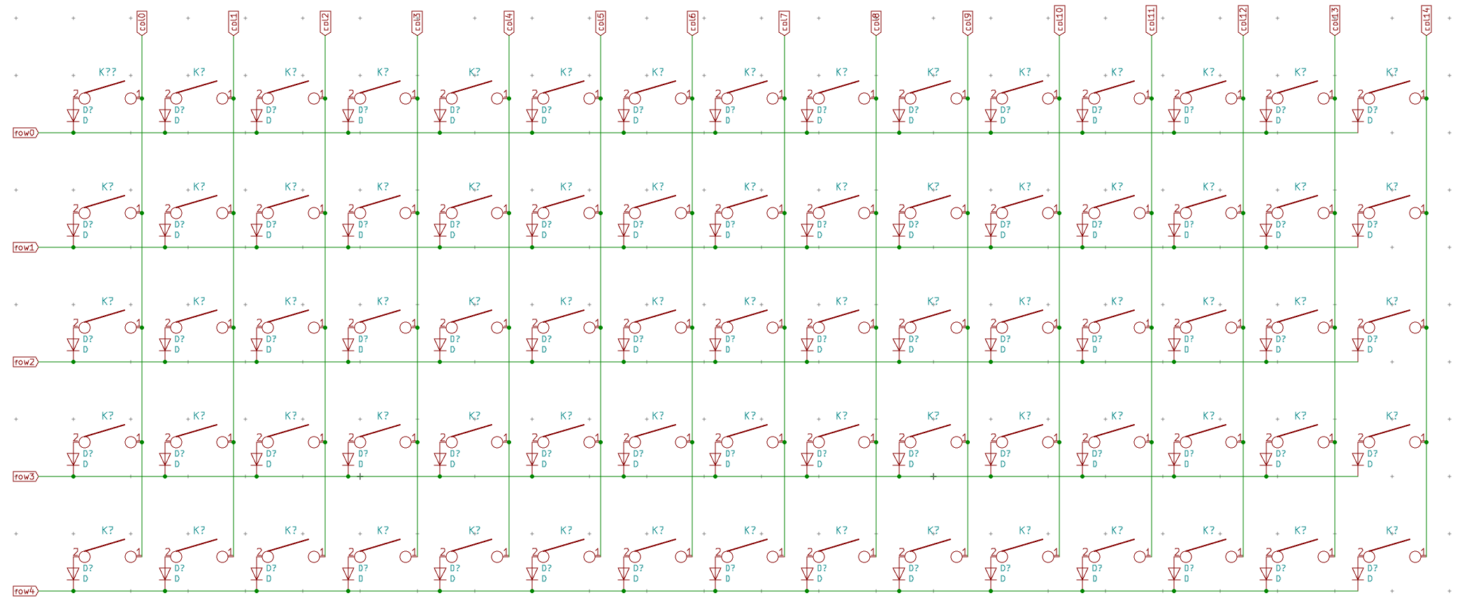
Next, edit all the row labels to make them row1, row2, etc. The columns also needs to be labelled. Start by adding a global label on the first column and label it col0. Use the shift-select trick to create a second one, then 2 extra ones, then 4 etc until all the columns are labelled.
Edit the labels so that they are labelled from col0 to col14.
Finally that was quick! But I suspect you’ve noticed there are too many keys in this matrix. I’m going to remove some of the extraneous switches so that the wiring would look like this if laid out on the physical layout:
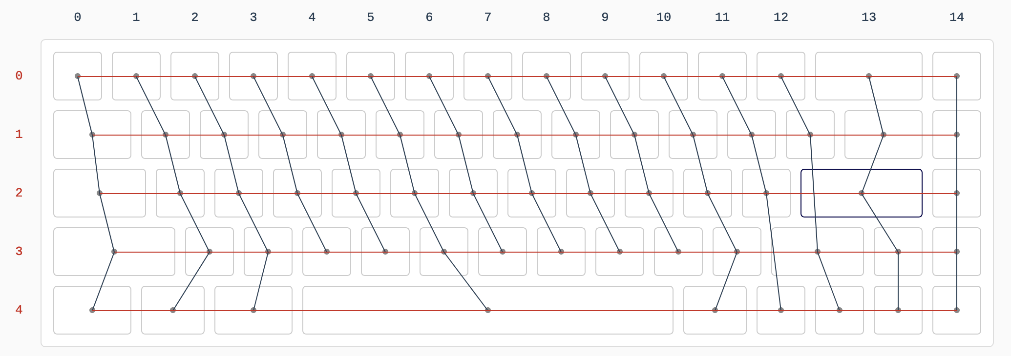
To eliminate the unneeded cells it’s as easy as selecting their switch and diode (and as less wire as possible) with a drag selection and pressing the del key.
The matrix should now look like this:
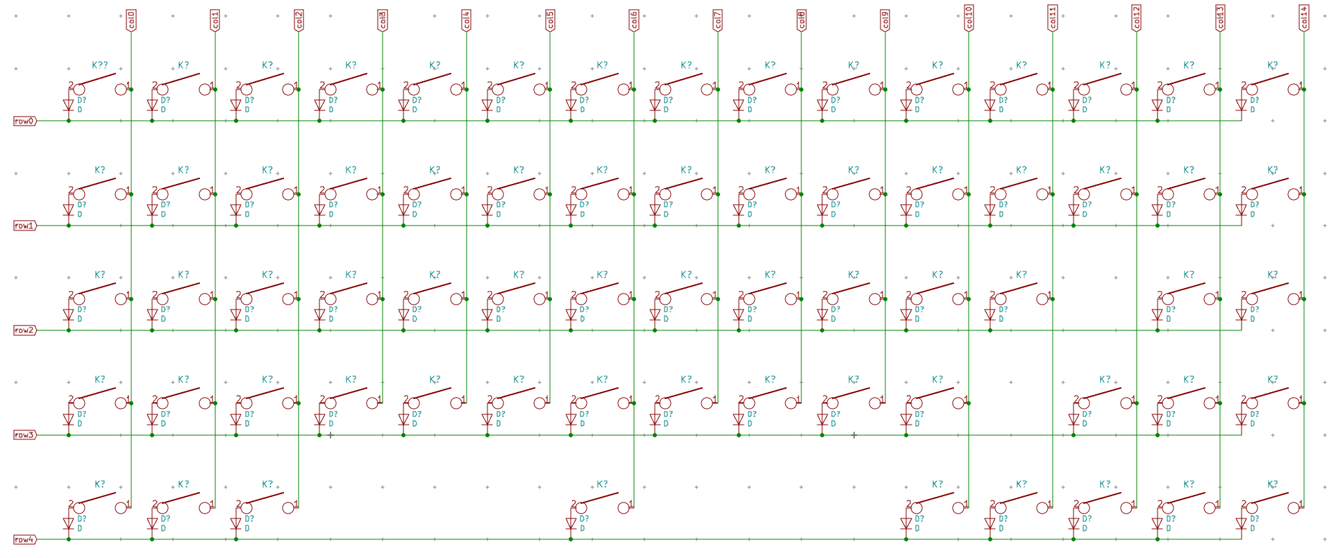
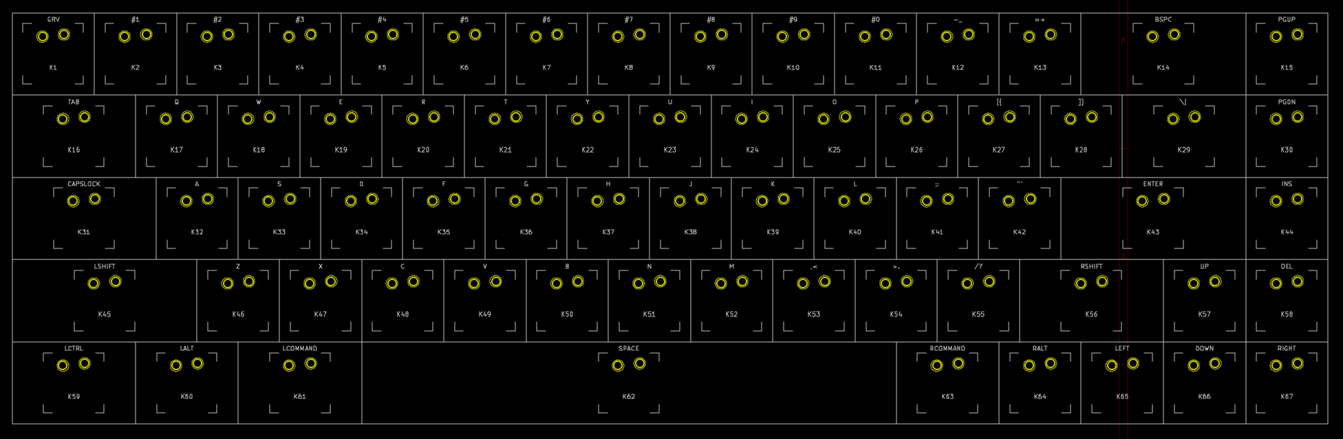
Now, I’m going to reference all the switches and diodes I just placed. Since I’m quite lazy, I’ll use the automatic referencing feature. If you want to reference switches by coordinates (ie first switch is K000, second one K001, but first of row1 is K100, etc), you’ll have to perform that manually (or write a script to directly modify the .sch file, or edit it with a text editor). I will just use increasing numbers in line.
Use the Tools → Annotate Schematics to open the annotation window:
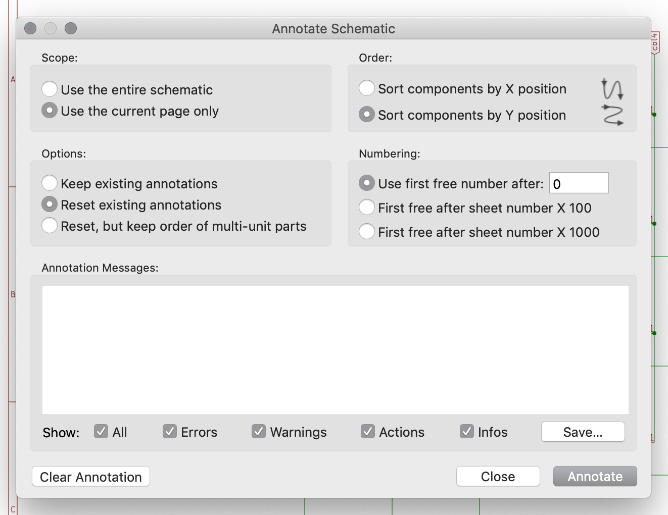
Make sure to annotate only the current page, and to Sort components by Y position. Once done, the matrix diodes and switches will have a proper unique reference identifiers. If you somehow failed, the same dialog can also erase all references (trust me, it’s easy to make a mistake, like for instance applying references to the whole schematics and not only to the current sheet).
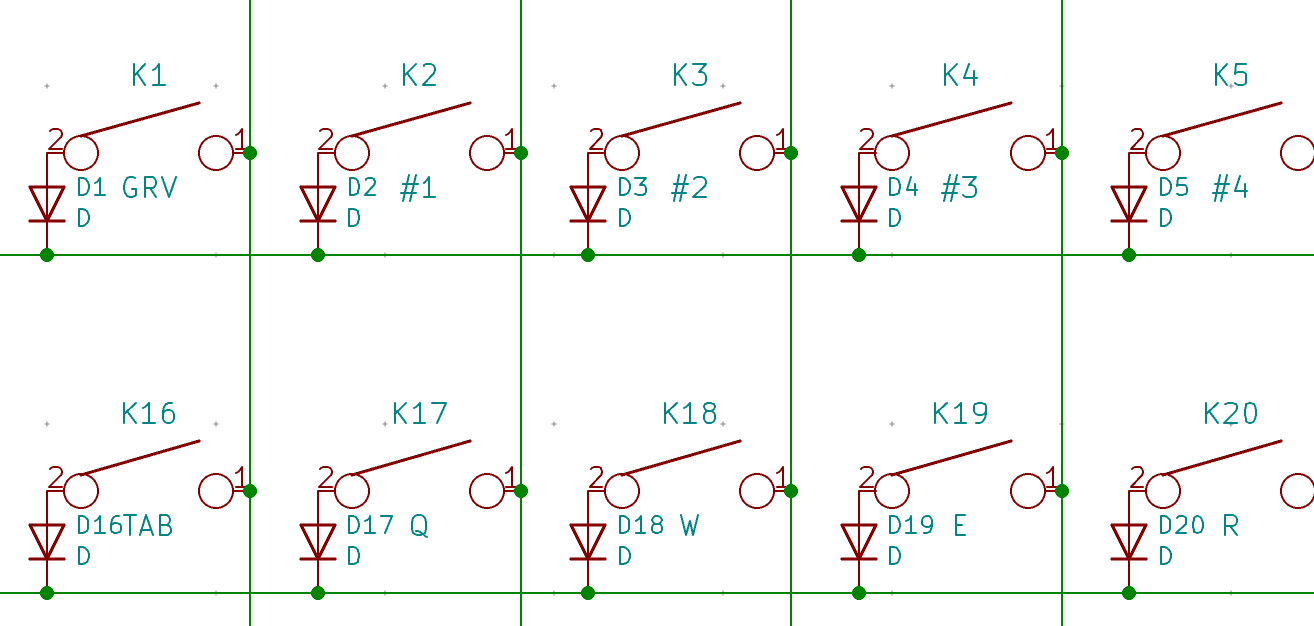
The next step is to label each switches with their key character or name (ie K1 will be GRV, K2 #1, K17 Q, etc). This will help when laying out the PCB, because the key name will be visible, compared to referring keys only by their identifier. I could have use the key name as the identifier (for instance K_SPACE, or K_ENTER), but Kicad wants each reference to contain a number which makes things look ugly in the end.
To assign key names to the switches, I’m going to use the Tools → Edit Symbol Fields window. This opens a new dialog that allows to group components by reference or value (or both) and to edit component values all at once:
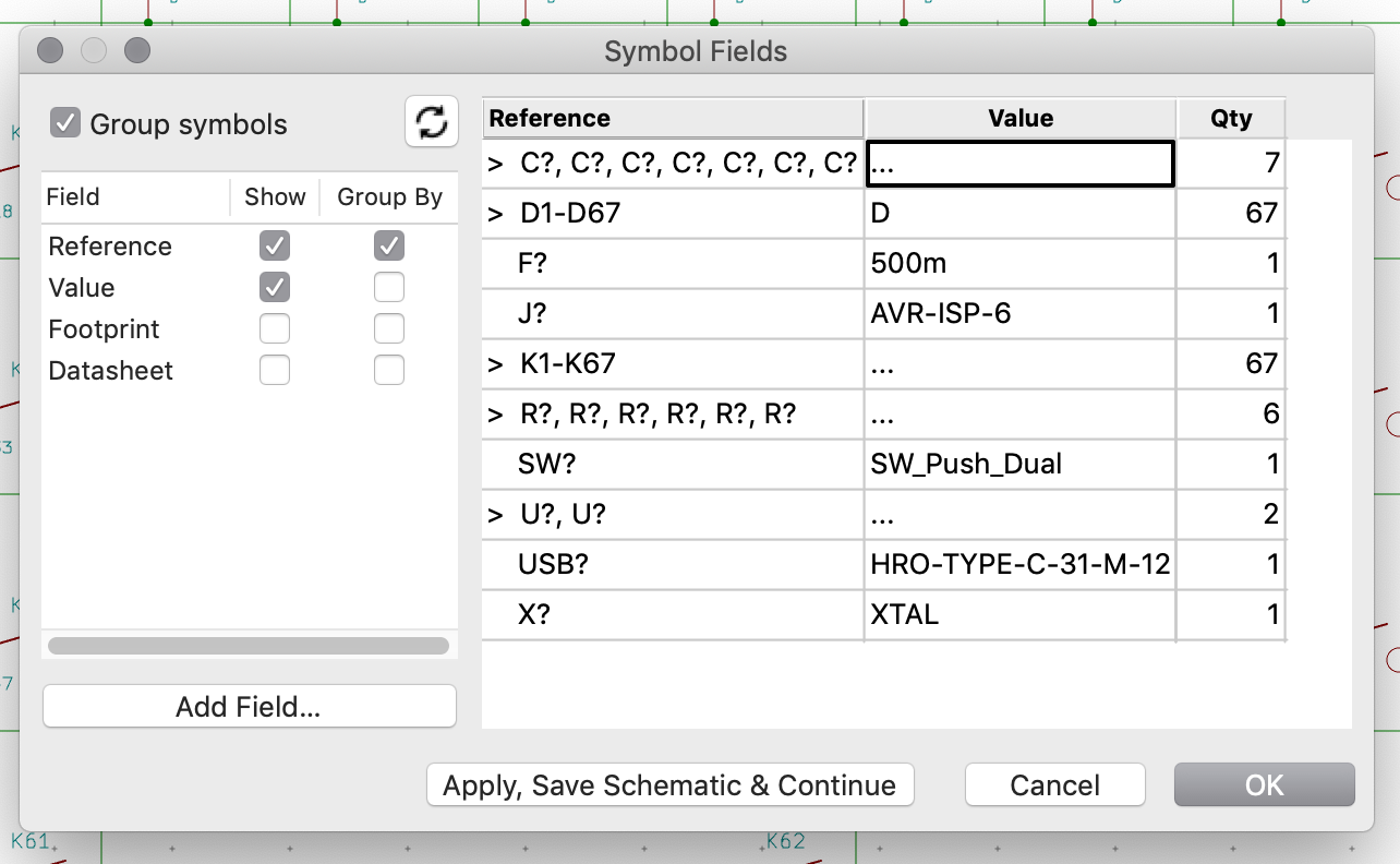
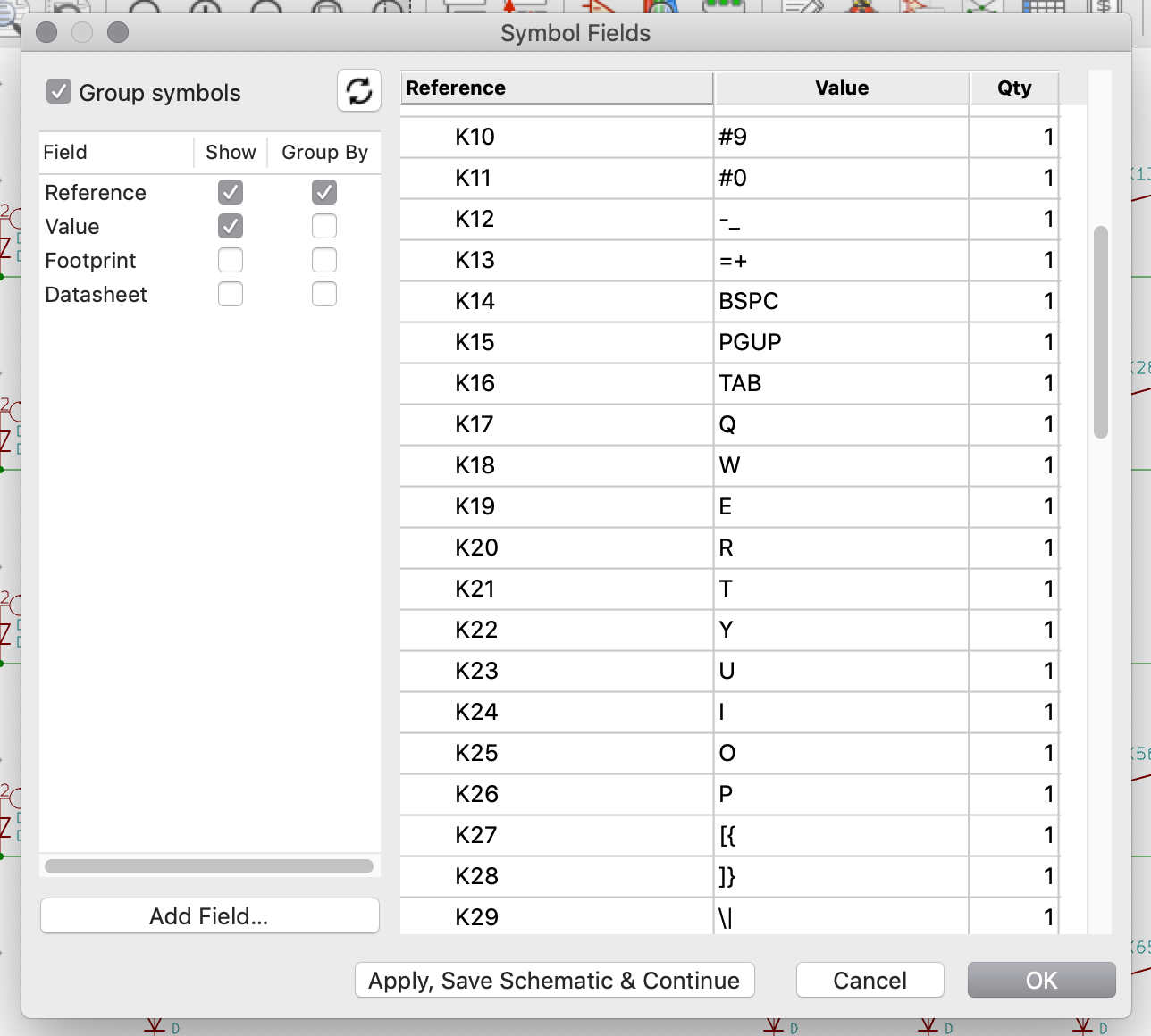
Open the K1-K67 group, and start assigning the correct key names in the value column to the switches in order:
Once done, the matrix itself shouldn’t be different than it was before. The key names don’t appear, because the KEYSW symbol have the value marked as invisible. Unfortunately it isn’t possible to edit this symbol with the Symbol Editor, toggle the value visibility and reassign the symbol to all the KEYSW in the matrix. Kicad allows you to do that, but doesn’t change the visibility of the existing symbols. If I want the key name to appear I will have to edit manually all the 67 switches to turn on their value visibility or edit the matrix.sch file with a text editor. I chose to alter the matrix.sch file with the sed command. Make sure to save the schema, close it and git commit the file and project before doing this:
sed -i -r -e 's/^F 1 "([^ ]+)" H ([0-9]+) ([0-9]+) ([0-9]+) 0001 C CNN/F 1 "\1" H \2 \3 \4 0000 C CNN/' matrix.sch
Reopen the root schema, then the matrix and you should see something like this:
The matrix is now finished. The perfectionist among us could move the key values or diode references so that they don’t collide (but remember I’m lazy).
The next step is to finish the main schema.
Prepare the MCU schema
Using the Tools → Annotate Symbols, I’m going to assign references to the main sheet (and only this one). Once done, to ease laying out the MCU on the PCB, I’m going to tentatively assign rows and columns to the Atmega32U4 pins.
To do that, I need to tell you a few rules about laying out our board:
- the
D+/D-signal form a differential pair. They need to be traced as directly as possible. - there’s only limited space available on the board between switches to put the MCU. Except behind the space bar where there’s no switch at all.
- the connections between the MCU and the matrix should cross each others as little as possible, thus the MCU should be oriented wisely so that left columns are assigned to pins to the left of the MCU and reverse.
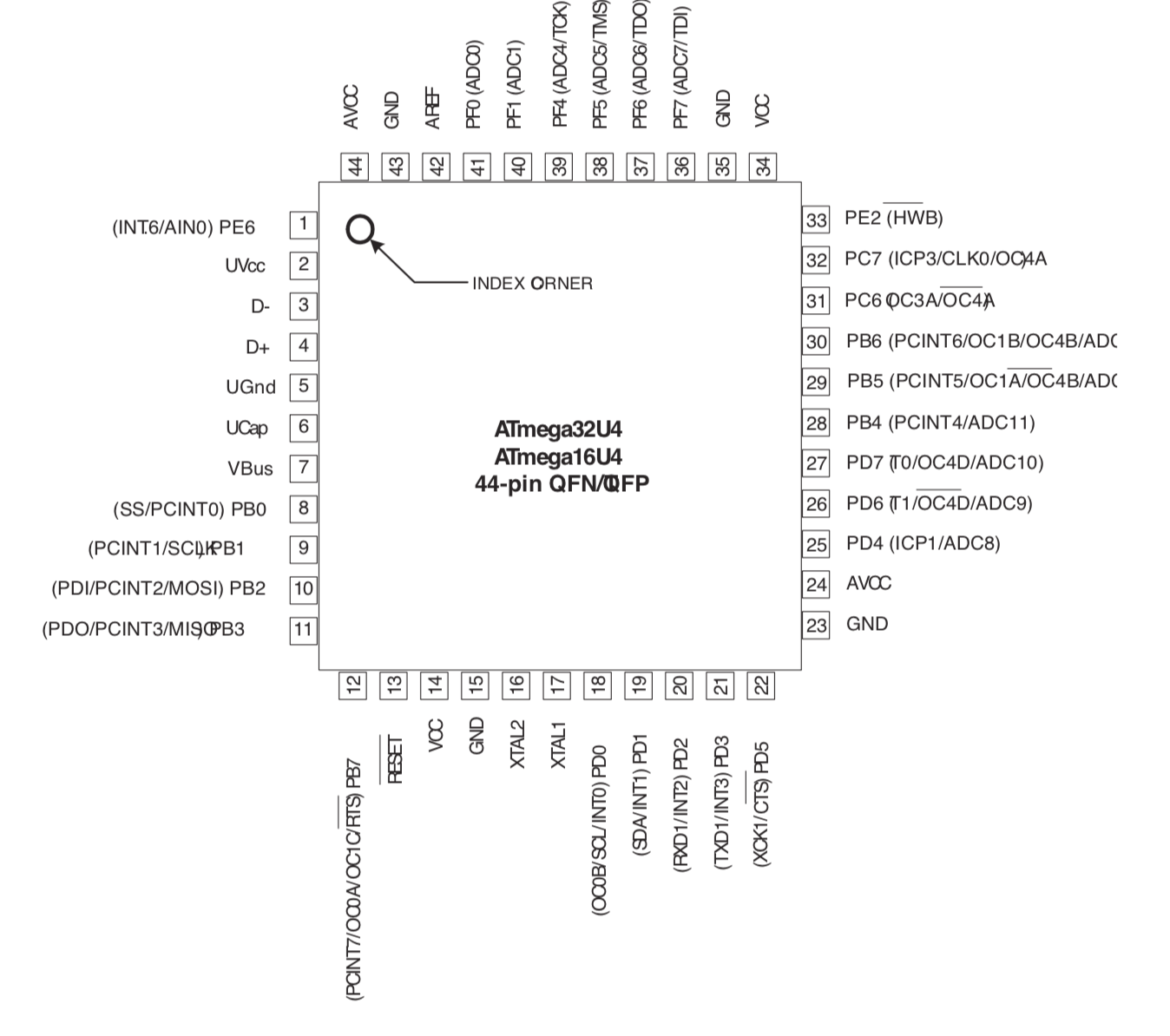
The physical layout of the MCU looks like this (it’s called a pinout):
With this in mind, if I want to minimize the length of the D+/D- paths, and considering that the MCU will stay behind the space bar at the bottom of the PCB and the USB port at the top, I will have to put the D+/D- pads face up. With this orientation, this means that:
- PF0, PF1, PF4, PF5, PF6, PF7 will be on the right
- PD0, PD1, PD2, PD3, PD5 will be on the left
- PD4, PD6, PD7 on the bottom left
- PB5, PB6, PC6, PC7 on the bottom right
Since the MCU will be on the back of the PCB, when looking from the top, then it is possible to assign col0 to col4 to bottom right pads (which will be left as seen from the bottom), col5 to col6 to the right pads, col8 to col14 to the bottom left corner. The rows can be connected on the PFx pins on the right.
Of course this is an attempt that will serve as a guide during the PCB layout. There are great chances that I’ll have to come back to the schema to reassign columns or rows to the MCU pins as I see fit.
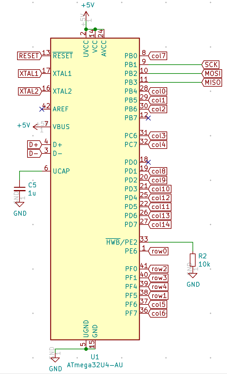
Here’s the schema with the rows and columns connected:
Check for errors
Before moving forward, I need to make sure everything is connected correctly. Kicad contains a tool called the Electrical Rules Checker that can help debug the schema connectivity. It is available in the Inspect menu.
The ERC shouldn’t display any error except a few about missing power. The ERC is complaining that our power nets (+5V, Vcc and GND) are not connected to real power sources. In fact all come out of the USB connector, but Kicad doesn’t know that this connector provides a source of power (or ground).
Hopefully there’s a way in Kicad to artificially tell those symbols are connected to a real power source. Those sources need to be connected to the special PWR_FLAG power symbol. Press the q shortcut to place a power symbol, and search for PWR_FLAG:
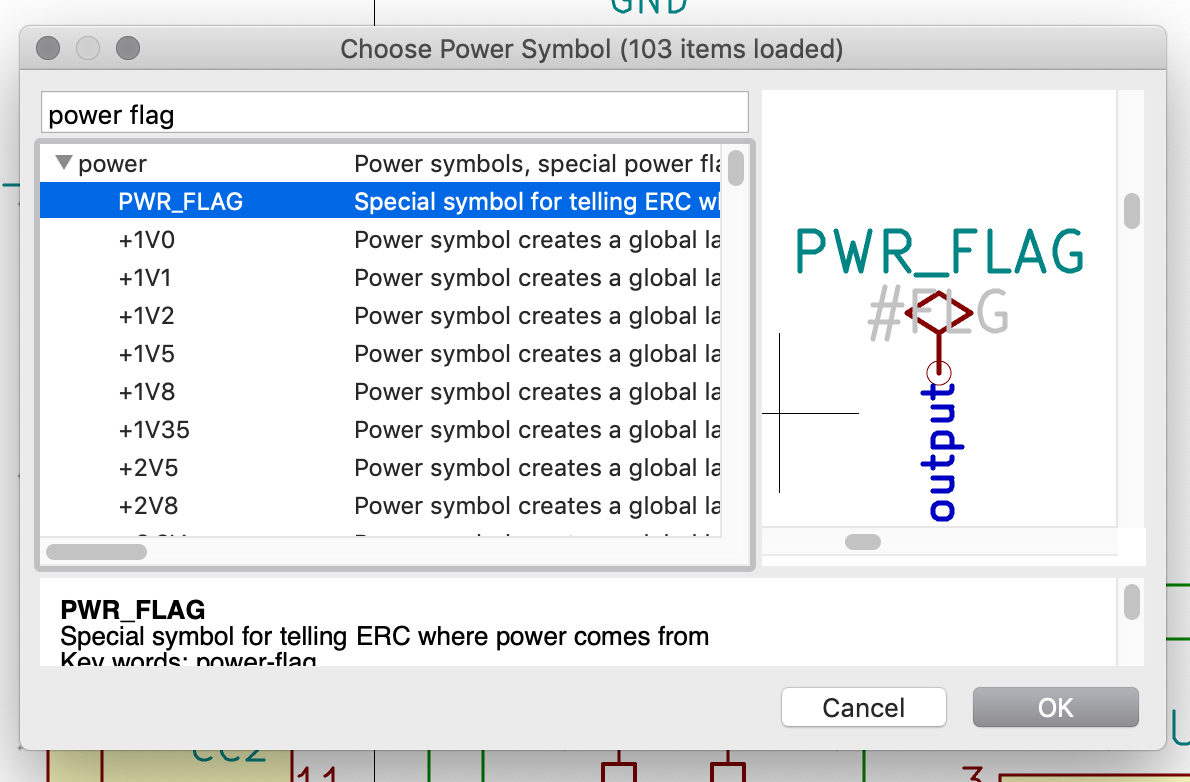
Place it on a wire connecting to GND, then place another one for Vcc and +5V:
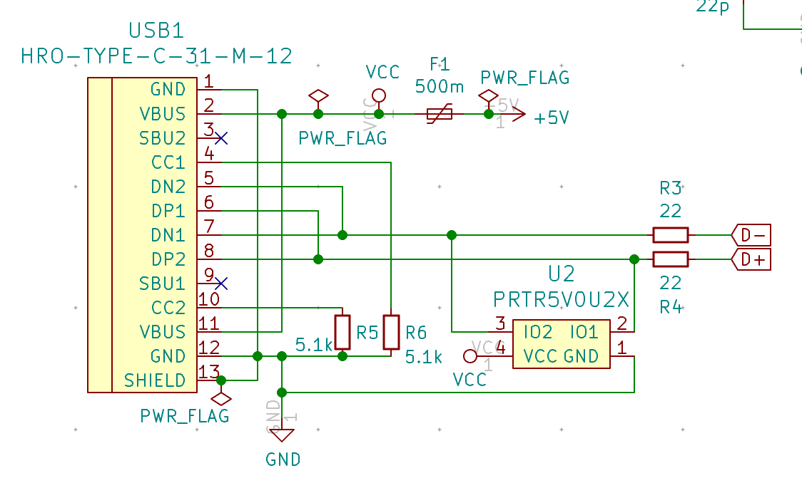
With those PWR_FLAG symbols in place, the ERC doesn’t report any errors anymore. I’m relatively confident the schema is right, but I suggest, if you also design a keyboard to double-check (and even triple-check) or ask someone in the community to check it for you (you wouldn’t want to receive a PCB that has a design flaw and that doesn’t work.)
Footprints
Up until now I’ve only talked about the electronic symbols. Serious things are still ahead. In this step, I’m going to assign footprints to the components of our electronic schema. A component footprint is a physical layout describing how the component will be soldered on the PCB (that’s actually a bit more than that). For instance, for a normal through-hole resistor, the footprint will have 2 holes surrounded by soldering pads spaced at a normalized distance, the same for IC or SMD components.
This project will only have SMD components (because they are much smaller). SMD components are soldered directly on the PCB. On the other hand I want to be able to solder them with my usual soldering iron and not a reflow oven or an hot-air gun. That means I have to choose SMD components that are big enough to be able to do that easily.
For passive components like resistors, capacitors, etc, there are several normalized sizes. From bigger ones like 1206, 0805, 0603, 0402, or even 0201. In fact this number represents the size of the component in inches (centi-inches even), so for instance 1206 means a length of 0.12 inch and a width of 0.6 inch (which makes them the large). It is relatively easy to hand-solder 1206 and 0805 components with a regular iron solder (I’ll explain the techniques in a subsequent post), but not so much for the smaller ones. Soldering such components requires a magnifying glass, a pair of tweezers and soldering flux at the very least.
Here’s the exact size of those different components:

For this PCB, I’m going to choose the 0805 (and not 1206 as I originally wrote) size so that it’s still easy to solder the components but allows routing traces around the MCU. Other components have different packages of different size too. For instances, diodes exists in SOD323, SOD123, MiniMelf packages etc. SOD123 packages are much easier to solder than MiniMELF packages, because MELF components are cylindrical (and they tend to roll or misalign easily).
Let’s assign footprints to the components now. Go to the Tools menu and choose Assign footprints:
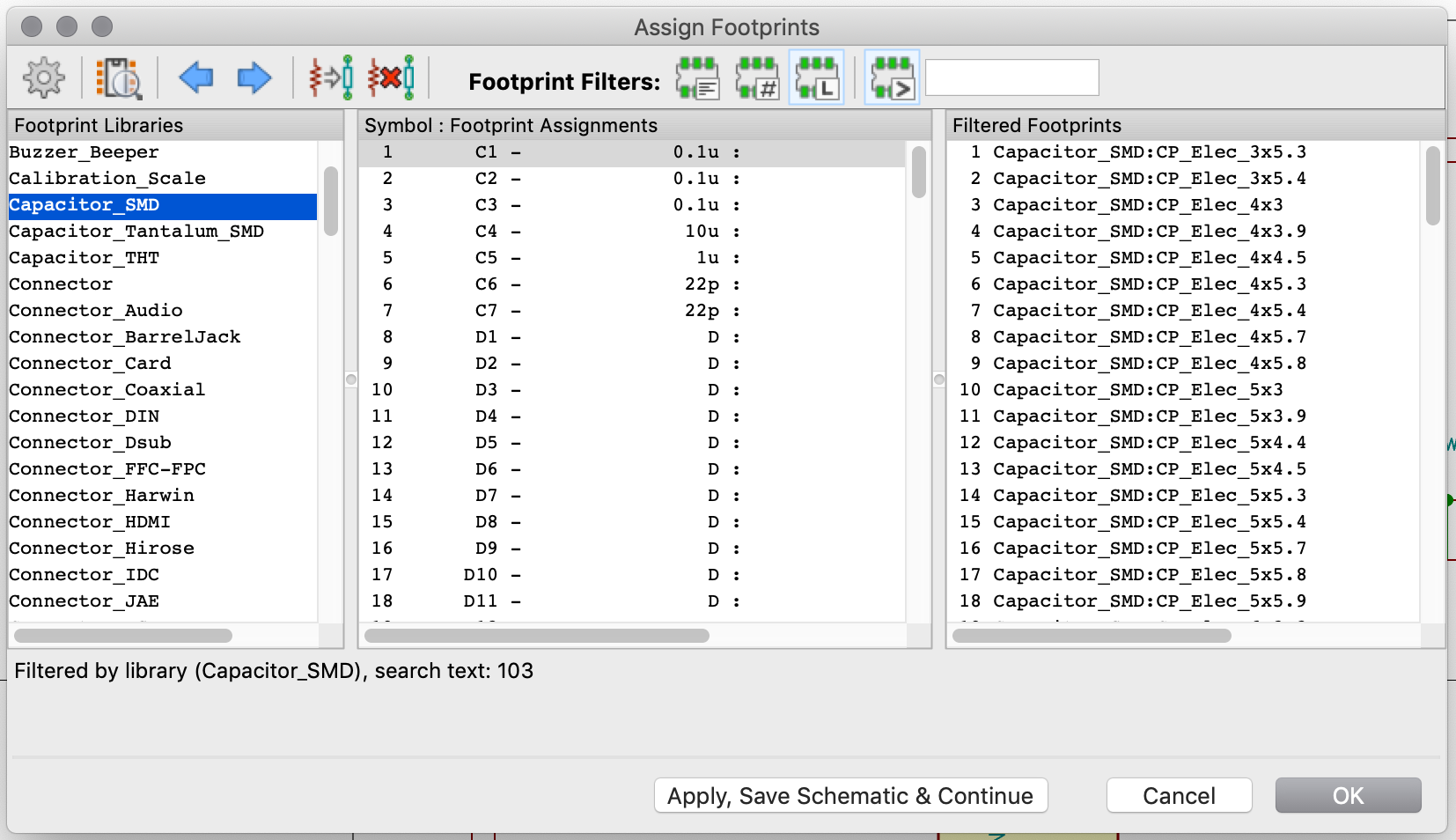
This dialog shows on the left column all the component classes, on the middle our components and on the right the individual footprints.
The task is to assign a given footprint to the references. With this, we can assign footprints in bulk, but it is also possible to assign a footprint to a given component directly from the schema by editing it (shortcut e).
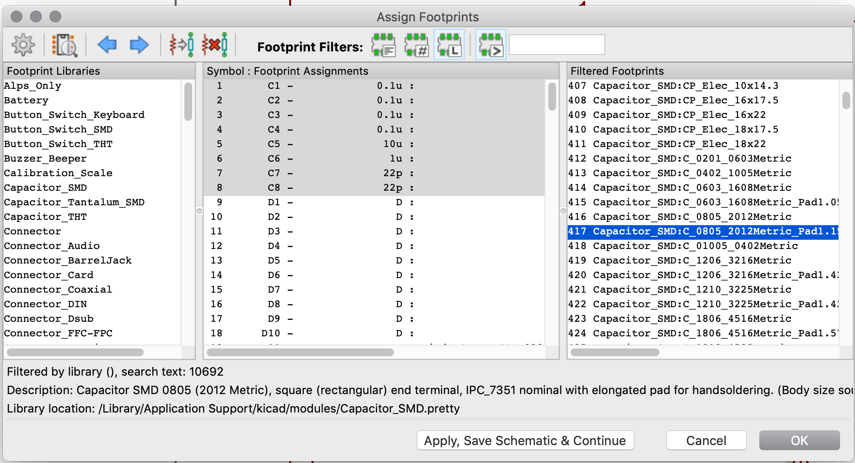
As said earlier, let’s assign a 0805 footprint to our capacitors. Select all C references at once, select the Capacitor_SMD class in the left column, and select the Capacitor_SMD:C_0805_2012Metric_Pad1.15x1.40mm_HandSolder footprint. I specifically chose the HandSolder variant, because the pads are a bit larger than a regular 0805 (in fact you can almost place a 0805 component in one pad of such footprint).
Do the same for the other components, and assign (use the search function to find the specific parts):
| Component | Footprint | Comment |
|---|---|---|
| Diodes | Diode_SMD:D_SOD-123 |
|
| 500mA Fuse | Fuse:Fuse_1206_3216Metric_Pad1.42x1.75mm_HandSolder |
|
| ISP header | random-keyboard-parts:Reset_Pretty-Mask |
|
K?? switches |
Alps_Only:ALPS-1U |
we’ll come back later to this |
| Capacitors | Capacitor_SMD:C_0805_2012Metric_Pad1.15x1.40mm_HandSolder |
|
| Resistors | Resistor_SMD:R_0805_2012Metric_Pad1.15x1.40mm_HandSolder |
|
| Atmega32U4 | Package_QFP:TQFP-44_10x10mm_P0.8mm |
it should already be assigned, but just in case |
| Reset push button | Button_Switch_SMD:SW_SPST_SKQG_WithStem |
|
| PRTR5V0U2X | random-keyboard-parts:SOT143B |
|
| USB Type-C connector | Type-C:HRO-TYPE-C-31-M-12-HandSoldering |
|
| Crystal | Crystal:Crystal_SMD_3225-4Pin_3.2x2.5mm_HandSoldering |
As an astute reader you might have noticed that I assigned 1U variants to all our switches, but that the library contained all the standard key sizes. Ai03 library contains footprints for the exact size of the various keys available on a keyboard which greatly simplifies laying out the switch footprints on the PCB. For the MX variants, larger keys also contains the PCB holes for the stabilizers. Because the references I attributed to the switches don’t tell which key it is, it’s relatively hard to assign the correct key size footprint directly from the Assign footprints dialog box. Instead I’m going to edit the handful keys larger than 1U directly from the schema, by pressing e on the switch symbol and assigning the following footprints:
| Key | Footprint |
|---|---|
| TAB | Alps_Only:ALPS-1.5U |
| CapsLock | Alps_Only:ALPS-1.75U |
| LShift | Alps_Only:ALPS-2.25U |
| LCtrl | Alps_Only:ALPS-1.5U |
| LAlt | Alps_Only:ALPS-1.25U |
| LCommand | Alps_Only:ALPS-1.5U |
| Space | Alps_Only:ALPS-6.5U |
| RAlt | Alps_Only:ALPS-1.25U |
| RShift | Alps_Only:ALPS-1.75U |
| Enter | Alps_Only:ALPS-2.25U |
| Backspace | Alps_Only:ALPS-2U |
| \| | Alps_Only:ALPS-1.5U |
To double-check, reopen the Assign footprints dialog box and make sure everything has a footprint.
PCB Preparation
The schema is now ready to be laid out on the PCB. The rest of the work will happen in the PCB layout program that is called pcbnew in Kicad. You can start it from the schema editor by clicking on the PCB icon in the toolbar.
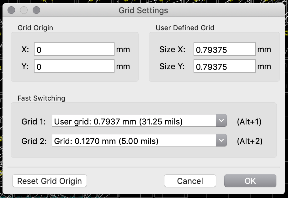
This will open the PCB editor with a blank view and grid. Do what ai03 suggests in his guide to setup the user grids: create a user grid settings with X: 0.79375 mm and Y: 0.79375 mm (make sure to be in mm, refer to ai03’s guide for the complete instructions):
Copper tracks have resistance. This means that a track has a voltage drop, power dissipation, and a temperature rise when current flows through it. The resistance is a function of the track length, width, thickness and of course resistivity of its material.
For signal tracks (like the matrix), there’s very few current involved, we can keep the Kicad default (0.25 mm or a bit less than 10 mils). The usual advice is to make the tracks as large as the design allows. A keyboard by definition has a large PCB. Since there’s no led nor any features other than the switches and the electronic components, this PCB will be reasonably empty. It’s a good news: we can make the power tracks as large as we need. By power tracks I mean in fact the +5V, VCC but also GND. In fact, GND is as important as the other power signals because it will carry all the return currents from the ICs, and thus is subject to as much current as the other power nets.
So power tracks are required to be larger, but what size do we have to use? Ai03 in his guide suggests 15 mils. This sounds right, but in fact there is a way to compute the exact track width. Unfortunately determining trace width is a complex science. The IPC has published a (paying) standard, IPC-2152. IPC-2152 publishes an abacus that allows to find the trace width based on projected current, copper thickness and temperature rise. Hopefully we can also use one of the numerous PCB trace width calculator.
Copper thickness on PCB is measured in oz/ft2 (looks like the metric system lost again). The default is usually 1 oz/ft2. If we have 500mA, default 1oz/ft2, and a maximum temperature rise of 5ºC (we don’t want the temperature to increase too much), the calculator returns 7.1 mils in open air, or 18 mils for inner layer trace. The IPC-2152 standards does it’s calculation with tracks spaced by 1 inch. This isn’t really practical for a real life PCB, so we might just want to aim for a smaller temperature rise (two parallel tracks at 500mA will increase temperature more than only one) to 2ºC (another solution could be to increase the projected current as if we had more current in one track simulating two close tracks). The result is a trace width of 12 mils.
Of course nothing is perfect, and the copper traces might contain debris or be etched. Any of those modifications will increase the trace resistance, and thus the temperature rise. Because this keyboard will be in a closed unventilated case, we need to limit the temperature rise as much as we can afford (remember that the MCU will also produce heat). Because of that, I’m going to add a safe margin and use 15 mils (as ai03 suggested) for the power traces.
Doing the same reasoning in reverse we could also reduce the size of the signal traces. Most manufacturer nowadays can do 5 mils (0.127 mm) traces. We have plenty of space on this keyboard PCB, and it costs the exact same thing if we do 5 mils traces or 10 mils traces, so let’s keep the default 10 mils.
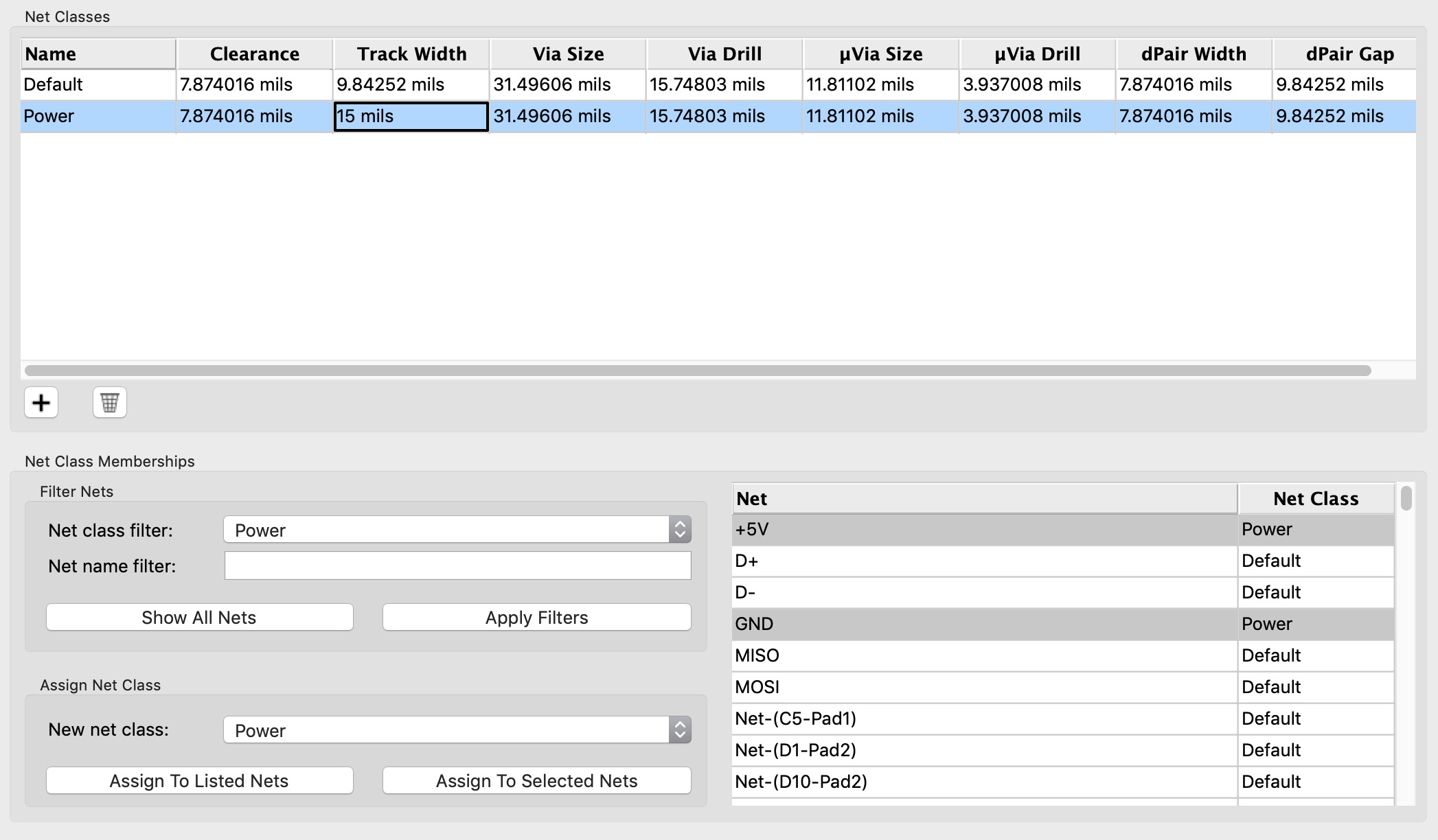
Kicad has a feature that allows you to declare trace width based on the net they’re built for (ie connections between components). This allows to automatically adapt the trace width depending on if the route is for power or signal. This can be done in the File → Board Setup dialog box, section Design Rules → Net classes.
Click on the + sign to add a class called Power, and adjust trace width to 15 mils (you have to be in inches mode to do that). Then in the bottom part of the dialog box, assign this power class to the VCC, +5V and GND nets:
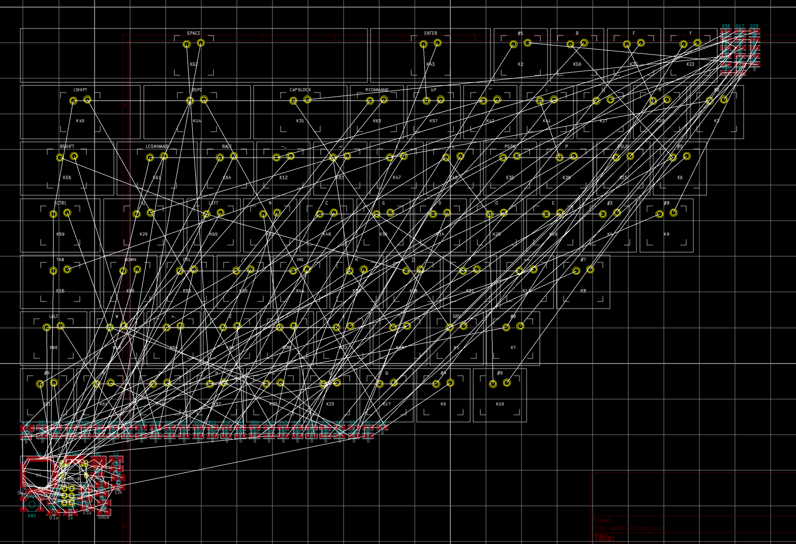
Finally, let’s import the components to the PCB by going to Tools → Update PCB from schematics…. This gives this pile of components:
You might notice all the components have been packed together (all the keys, all the diodes, etc). If you zoom in on the components, you’ll notice that their pads are all drawn in red. This means those components are laid on the top of the PCB. This is the perfect time to talk about PCB layers.
A PCB is a dielectric board usually made from FR4 fiberglass. Copper planes are sandwiching this board, on which the traces are drawn. There can be one layer, 2 layers (one at the top, one at the bottom), 4 layers (2 on top separated by a dielectric substrate, and 2 at the bottom), 6 layers, etc. Each couple of layers increases the manufacturing price. For this keyboard, a 2 layers PCB will be enough.
Kicad defaults to two layers boards (you can add more if needed), one on top (the red one) and one on the bottom (the green one), they are respectively named: F.Cu (Front copper), and B.Cu (back copper). But Kicad also defines other layers:
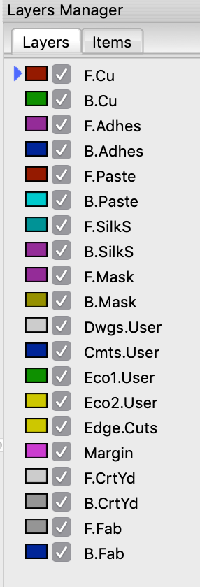
Here is a table summarizing their usages:
| Layer name | Type | Usage |
|---|---|---|
| Cu | Technical pair | Copper layer for traces |
| Adhes | Technical pair | application of adhesive to stick SMD components to the board prior to soldering |
| Paste | Technical pair | mask to place solder paste for reflow soldering |
| SilkS | Technical pair | where the components are drawn |
| Mask | Technical pair | defines the areas free of soldermask like component pads |
| CrtYd | Technical pair | show how much space a component physically takes |
| Fab | Technical pair | documentation for manufacturing |
| Fab | Technical pair | documentation for manufacturing |
| Edge.cuts | Independent | the board shape |
| Margin | Independent | to define a safe margin for edge cuts |
| Dwgs | Optional | can be used for instructions, drawings. Some footprints use them |
| Cmts | Optional | can be used for instructions, drawings. Some footprints use them |
| ECO1/2 | Optional | user specific, never used in footprints |
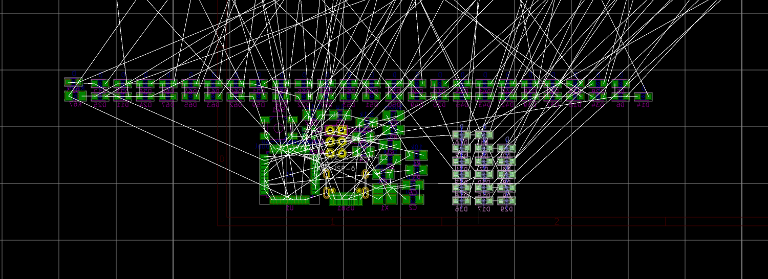
Since this PCB will have two layers, it would be possible to evenly spread the components on both layers. Since there are much more room on the back (all the switches take space on the top), it’s preferable to put all the SMD components on the back (bottom layer). Also, putting all the components on the same layer would reduce the manufacturing costs if I wanted to order soldering. Note that this will also reduce the number of vias (a via is a hole in the PCB that connects electrically two layers).
First let’s move all SMD component footprints to the B.Cu layer. To do that drag select the components and press the f shortcut (to flip them to the other face). If they get placed on the way or far away, press m to move them closer.
Laying out components
The most difficult task in designing a PCB is routing the copper traces between components. Those traces should be carefully designed to prevent EMI (I’ll talk about that in a subsequent post), not cross layers too many times etc. Routing is an iterative process that is very time consuming, and can be considered as an art (at which I’m a newbie, you’ll see that soon). But before we can start routing the PCB, we need to place the components. Laying out the component is more than half of the routing work. Components badly placed can make routing hard or impossible.
Some components can’t be placed anywhere, think for instance of the switches that need to be placed where the keys will be. Same for the USB-C connector. Then other components might have constraints that also mandate where they are, for instance the decoupling capacitors that need to be close to the MCU to be effective.
Placing the switches
I’m going to start with the key switches because that’s them that will define the size and aspect of the PCB. Let’s switch to the User Grid 0.7937 mm which has been designed to place switches. This grid is 1/24th of a key. The task is to move every switch footprint in the order of the layout of the final keyboard, starting with the GRV key. With this User Grid in place, the switches will snap together perfectly. It is also possible to use the arrow keys to move the components in place.
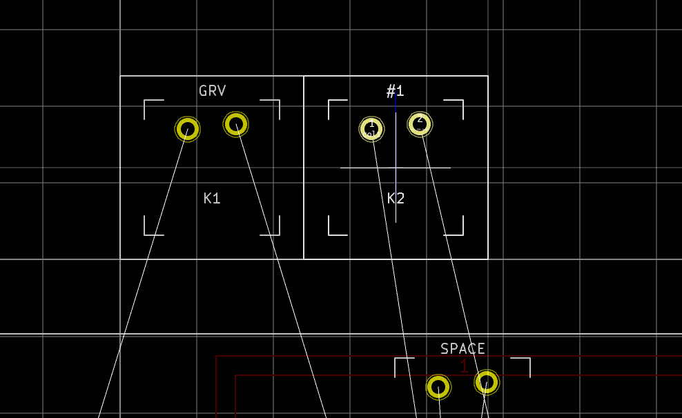
Keep going until all the keys form the layout. Note that the key name (which we put in the component value earlier) appears on the footprint. This simplifies the placement of the switches.
If you struggle to find a key, you can use the Find functionality (Ctrl-F) and enter the key reference. Even better use the t shortcut to activate the Get & Move Footprint feature, enter the reference, then move it to the right place.
Here again it is easy since we’re laying out the keys in order of increasing K? reference (from K1 to K67). Make sure all switches outer white bounds are aligned when placing a new key next to an already placed one. Their borders should only form one thin white line. It might be easier to hide the rats-nest while placing the switches (there’s a button in the left vertical toolbar to do that).
In no time you’ll get the whole matrix properly aligned:
In the process of aligning the keys, I noticed that I misattributed the footprints of two keys. To correct such mistake, you need to go back to the schema, change the footprints to the correct ones (by editing the components). Next go back to the PCB editor and click on the Tools → Update PCB from schematics…. In this dialog box, make sure to select the Update footprints and the Reassociate footprints by reference method. The misattributed footprints should be corrected automatically.
Placing the diodes
The next step is also quite tedious. It consists of moving all the diodes to their parent switch positions (by using the t shortcut). Still with the switch User Grid, start with D1, move it to the K1 position, rotate it as you see fit with the r shortcut. Do the same for D2 and so on:
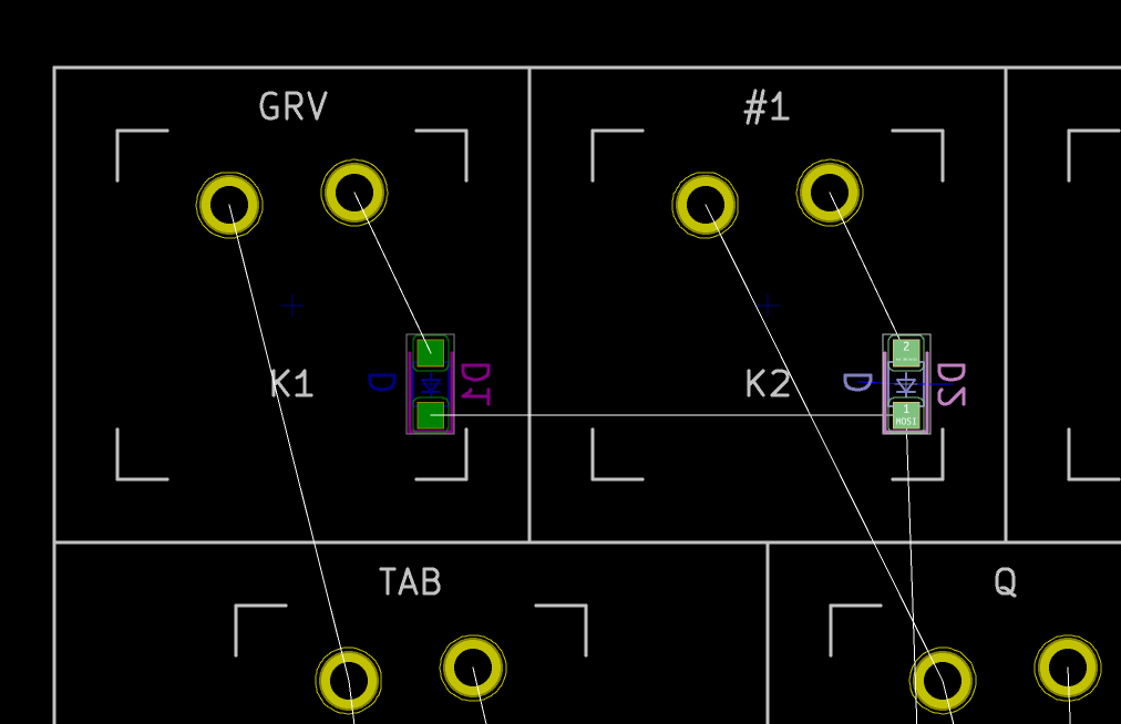
It’s best to do this part with the rats-nest visible. The rats-nest is the forest of white lines that connect all pads part of the same net. It’s a visual help used during trace routing. In the diode layout phase it also helps visualize rows and columns. For instance in the picture above, D1 pad 1 and D2 pad 2 are connected to form a row.
Once done, the result looks like that (the entropy has greatly declined !):
USB-C Connector
The next components to lay out is the USB Type-C connector and its associated components (like the fuse, the ESD protection IC, etc).
There are different schools regarding where to place the USB connector. I find centered connector to be more appealing visually. Still with the switch User Grid settings, move the connector to the center top of the board (which happen to be between the 7 and 8 key):
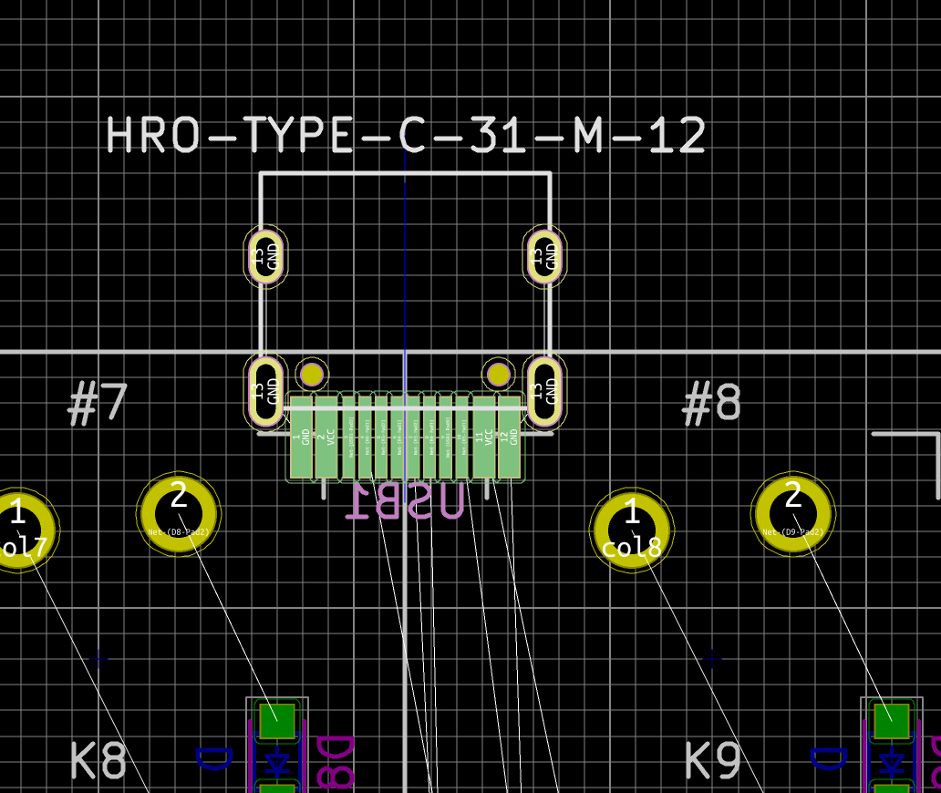
Since the footprints hotpoint is exactly at the center, and thanks to the switch User Grid Settings, it is easy to perfectly snap in the connector between two keys.
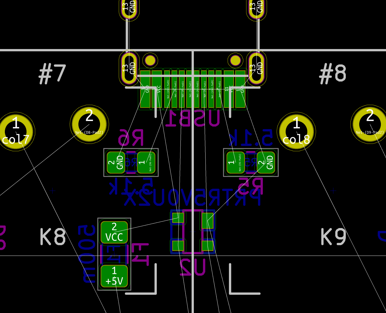
Next, we’ll move the components that needs to be close to the USB connector there. It means both 5.1k resistors, the PTC fuse and the ESD protection device. Notice how I carefully placed those to minimize the number of nets crossing:
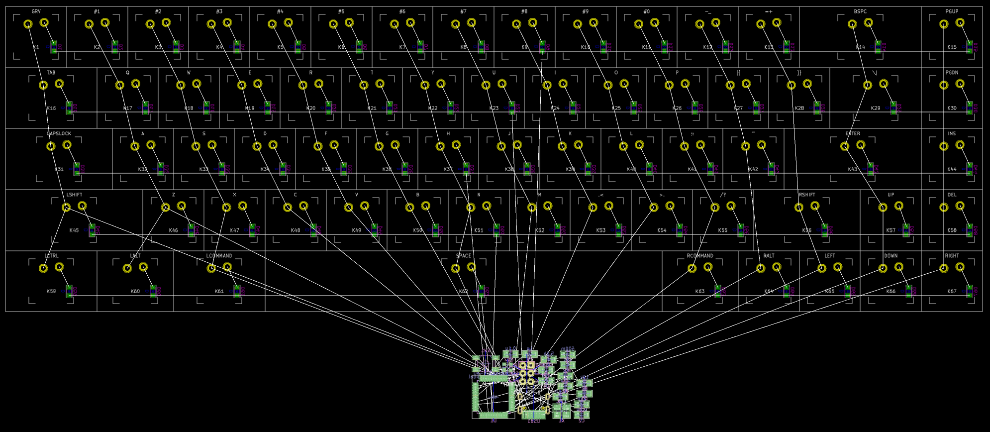
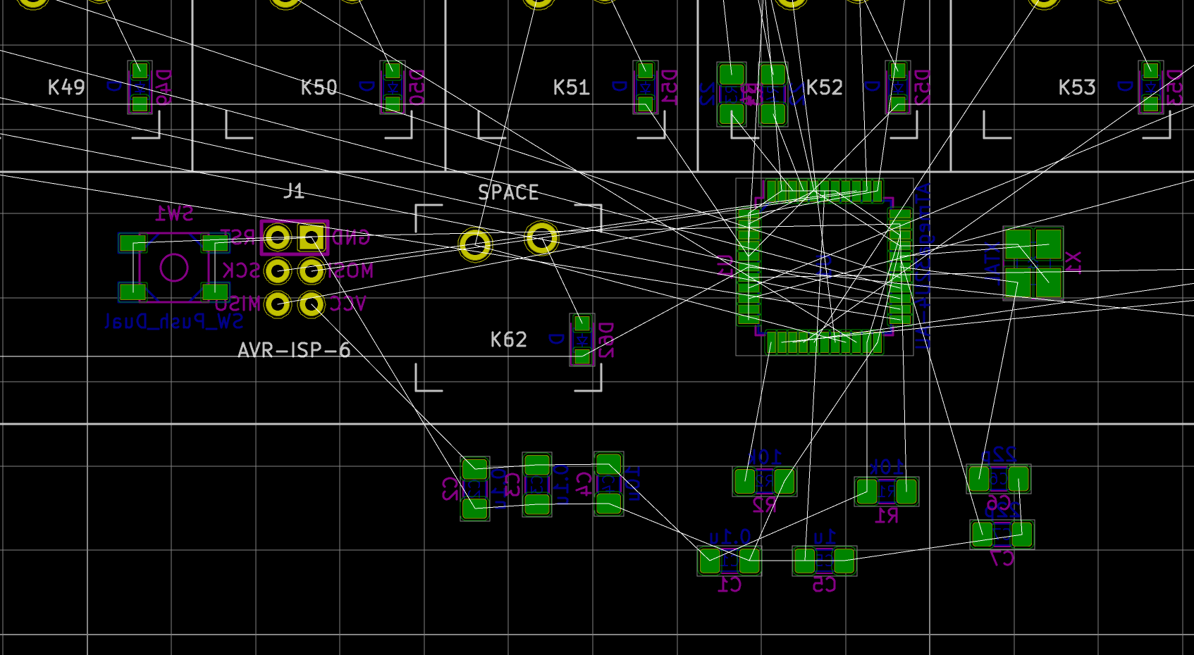
The MCU
Now, I need to take care of the MCU and the components that are connected to it. The MCU is quite large, but hopefully there is enough room between the space key switch and the other switches. Ideally we have to route the D+/D- differential pair with the shortest path possible (to control the USB data-lines impedance). The crystal also needs some room. It looks like the best way is to orient the MCU with the D+/D- pins face up and the crystal to it’s right. Of course, things will probably change when I’ll start routing:
Around the MCU, there are so many nets that it might be hard to see what’s connected to what. At any time it is possible to highlight a net by using the Highlight net function (shortcut \`). For instance to better see the nets around the crystal:
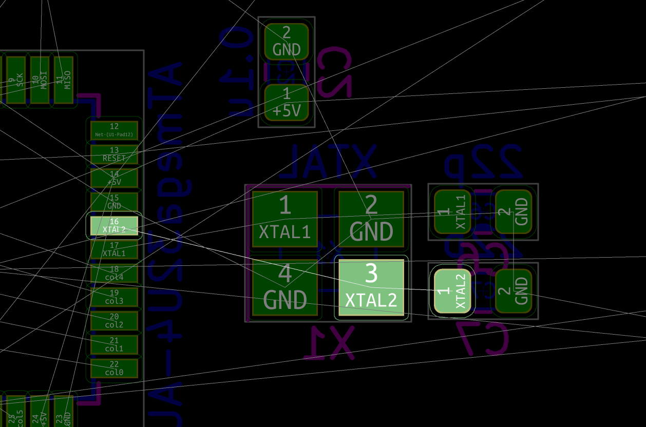
The crystal needs to be connected to the two 22pF capacitors and the two XTAL1 and XTAL2 pads on the MCU. The following arrangement allows to take advantage of the free space around the MCU while minimizing the number of crossing nets and leaving room for routing the matrix around:
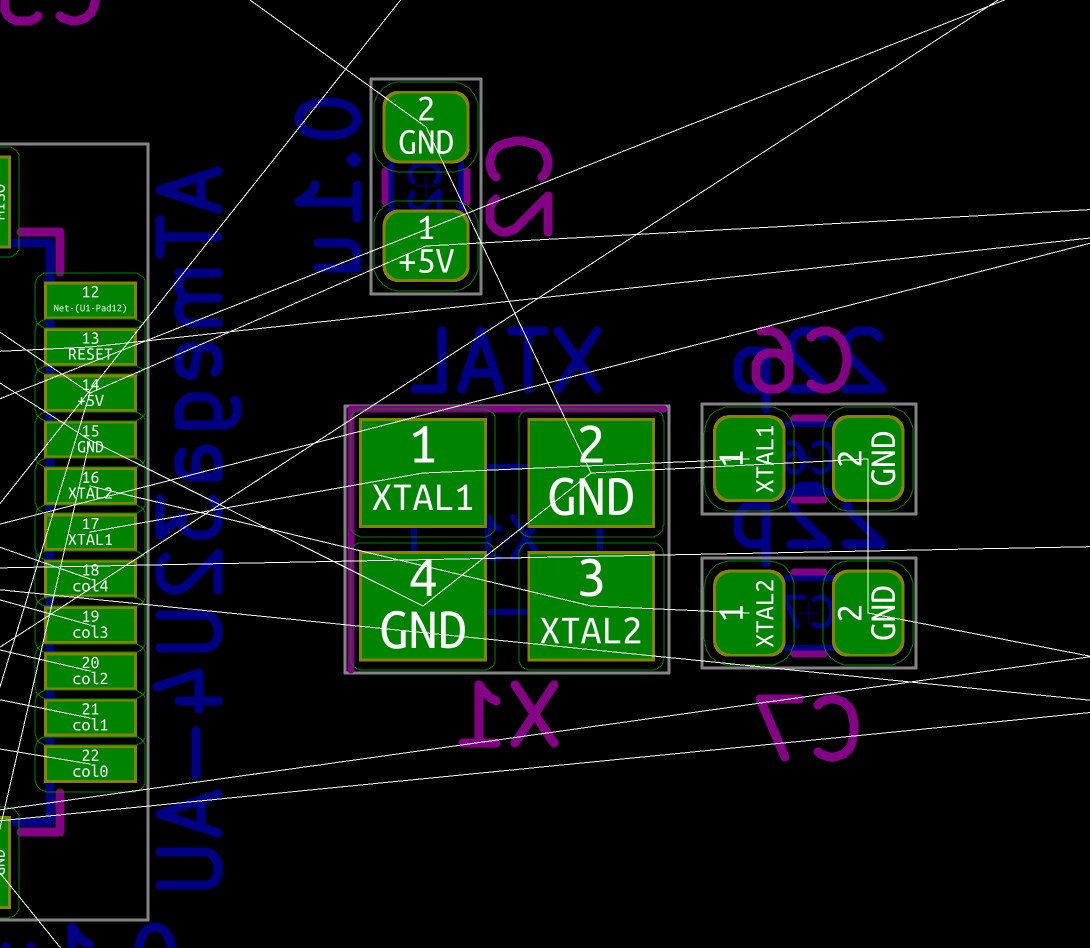
The D+/D- differential pair (the USB data lines) requires two 22 ohms resistors to make sure the USB bus is terminated with the correct impedance. Those have to be placed as close as possible to the MCU. We can orient them in the direction of the USB-C connector:
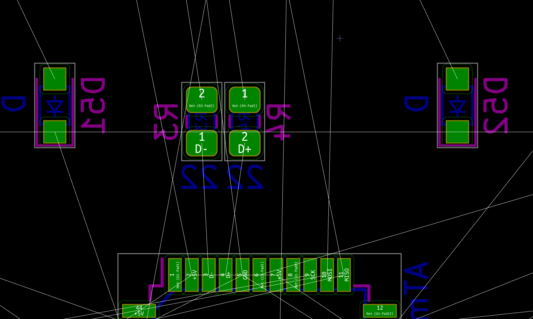
The next step is to add a decoupling capacitor for each VCC pad of the MCU. We’ll keep the 10uF capacitor close to UVCC and VBUS as I explained in the first part. The rest of the 0.1uF capacitors will be moved close to the other VCC pins. The idea again is to minimize the number of nets crossing while still leaving room for routing traces. We also do the same for the RESET pull-up resistor, the UCAP capacitor and the HWB resistor, and finally the reset push button:
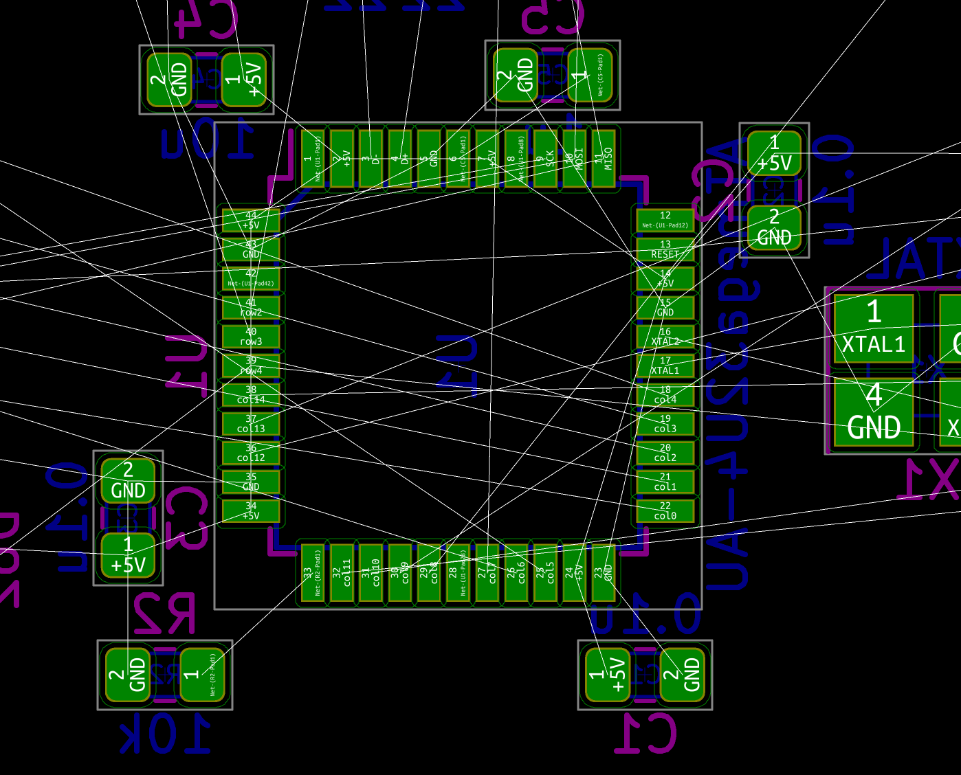
As said earlier, this is a tentative layout. When I’ll start the routing, there are very good chances that I’ll have to move things a little. Note also that I haven’t placed the ISP header. I’ll do that during routing, because the matrix might not be hooked exactly like we did above in the end, and I might reuse the MISO, MOSI or SCK pins for the matrix.
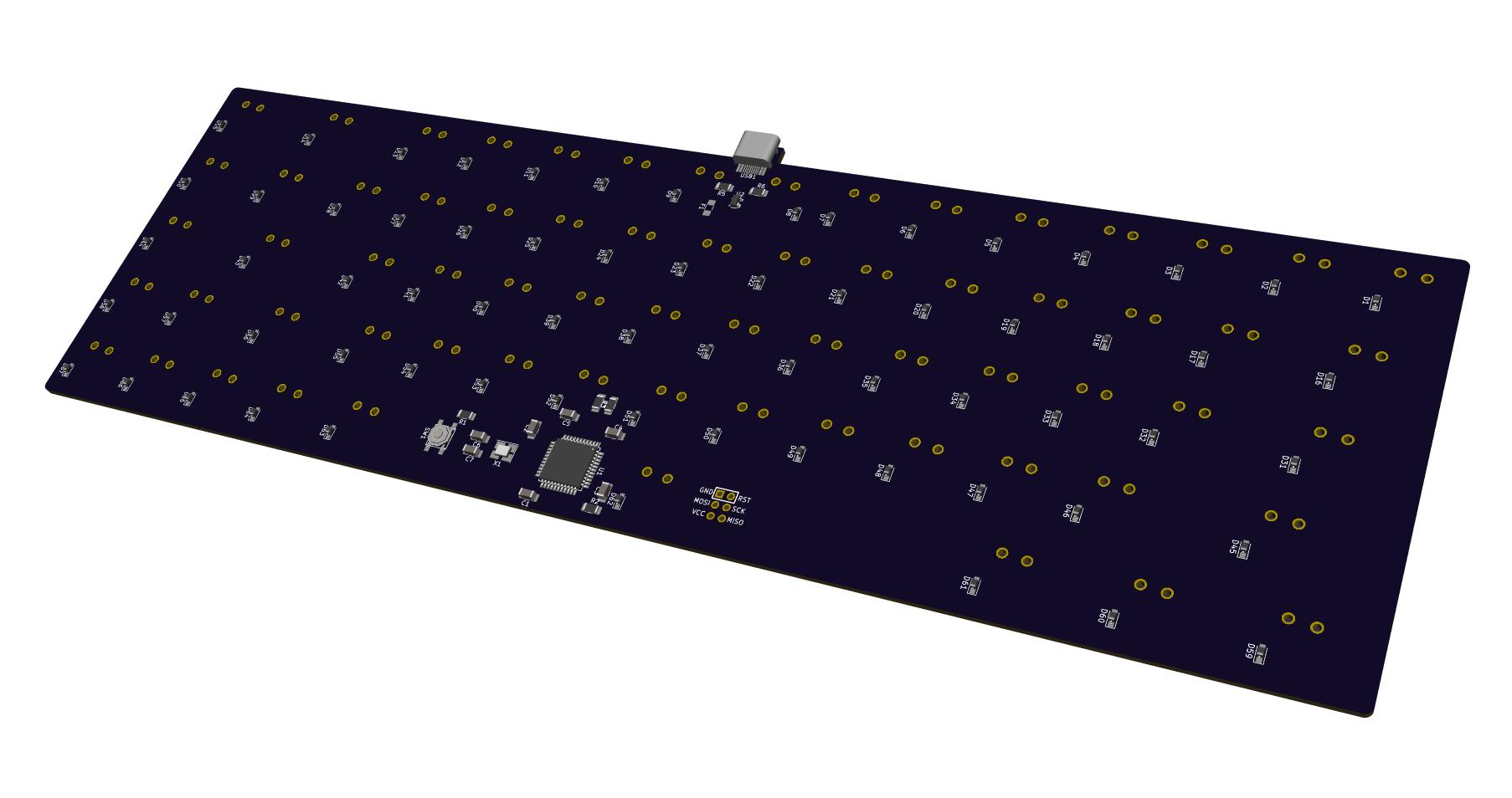
The board now looks like this:
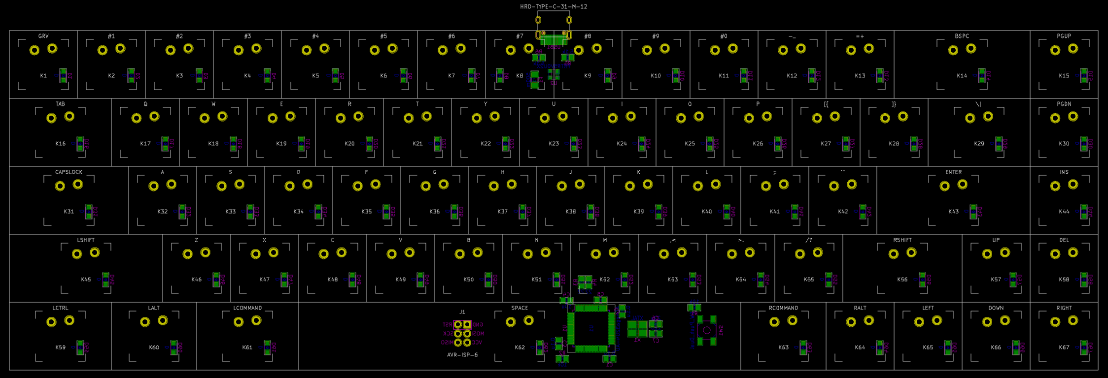
Notice that all components are now placed inside the switch footprints, thanks to the SMD components small size.
Cutting edges
Now that everything is approximately at the right place, we can design the PCB border. In order to do that, I’m going to draw the contour while being in the Edge.Cuts layer. This will let the manufacturer know where the board should be cut. This can be used to give specific forms to the PCB. In this case, I’m going to draw the border exactly on the key bounding boxes, including the USB connector. The HRO-TYPE-C-31-M-12 connector has four through-hole pins that needs to be soldered which means the PCB must extend under those (this will help secure the connector and prevent it to become lose while connecting/disconnecting cables frequently).
Let’s start at the top-right corner (any corner will work though), select the Edge.Cuts layer and the Arc tool. Switch to the switch User Grid settings if you’re not in it and click in the middle of the top right corner:
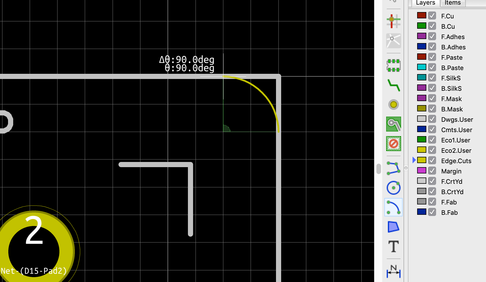
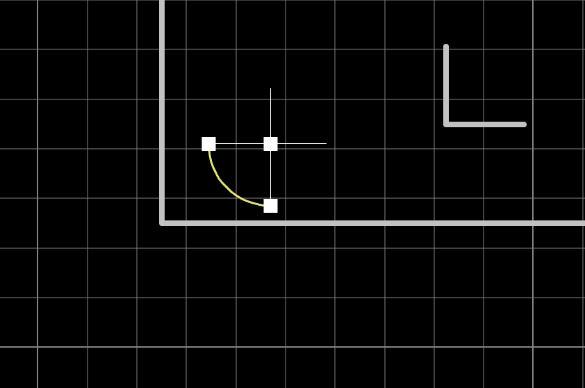
Select the arc that just has been drawn and Copy it (Ctrl-C) by clicking on its control points. Then paste the copy (Ctrl-V) and move it to the bottom-right corner (or any other corner). Rotate it by pressing r until it has the correct orientation and place it in the corner:
Repeat for the two remaining corners. Before adding the edge lines, I believe it’s easier to prepare the USB connector. Draw an Arc on the left part of the connector and continue it with a line:
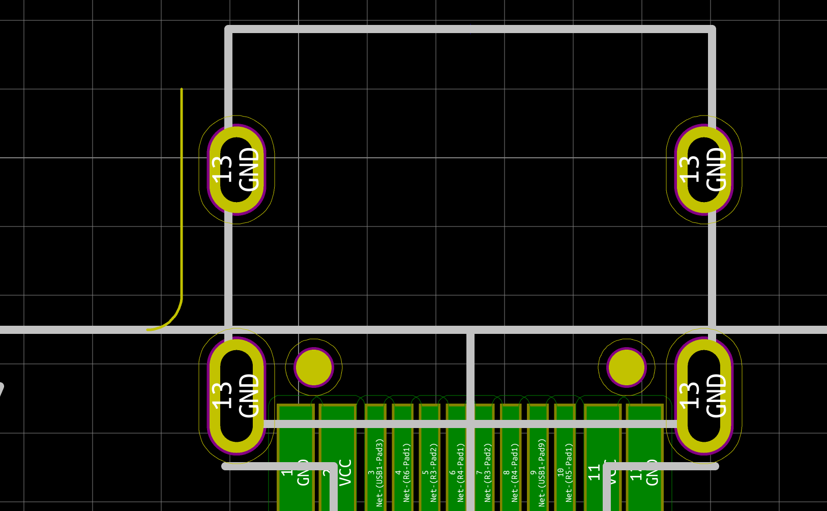
Then the draw the horizontal and right vertical edge:

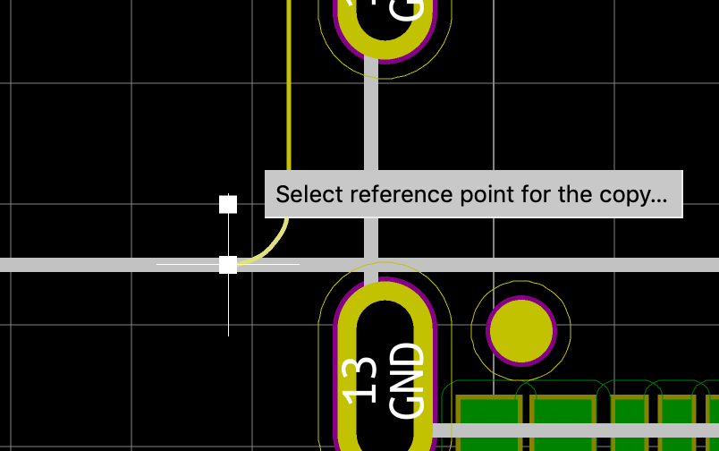
And finally copy the left arc (make sure to click the the bottom left control point):
Next, move the arc to the right part of the usb and rotate it (r):
Then finish the border by drawing Lines connecting all the rounded corners:
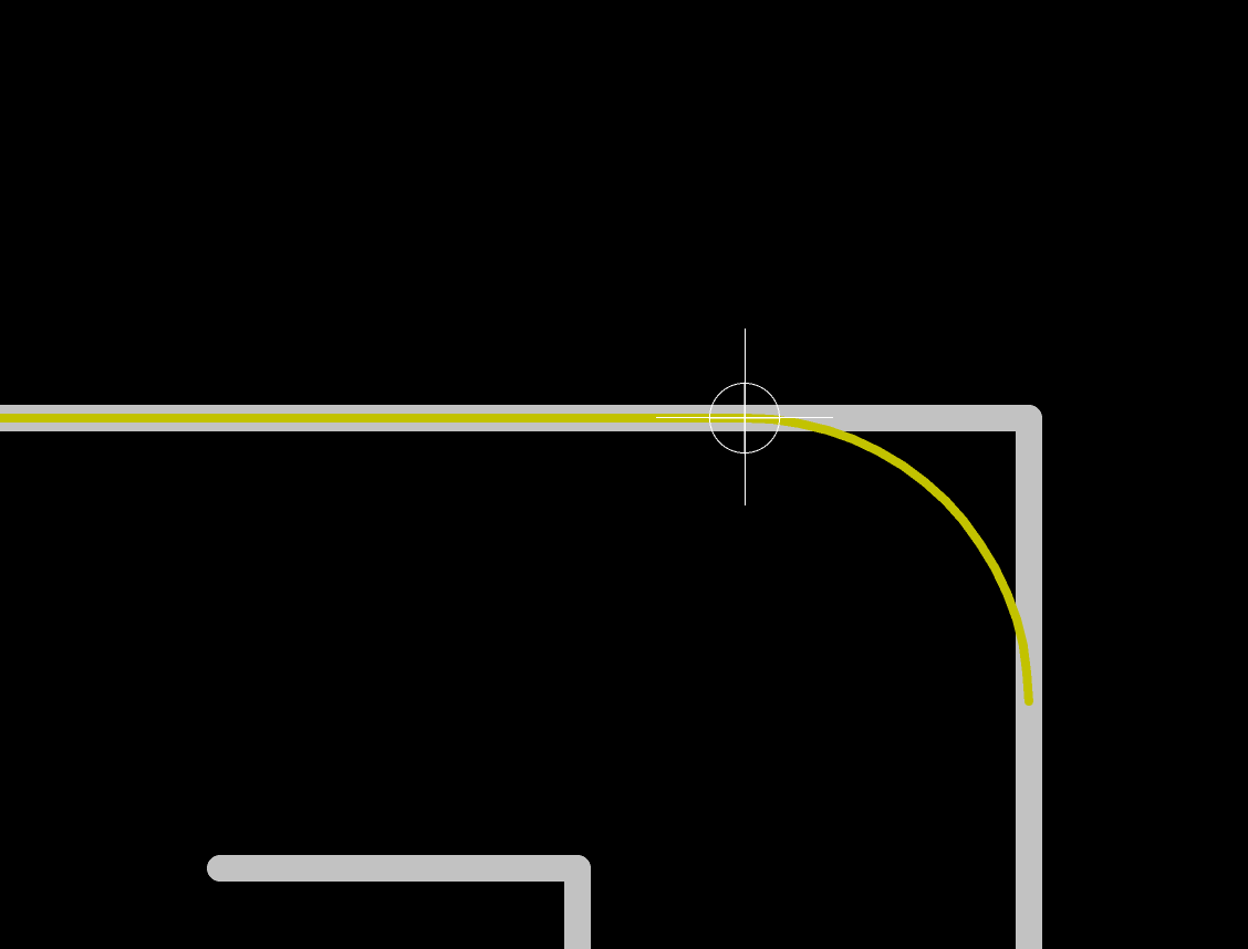
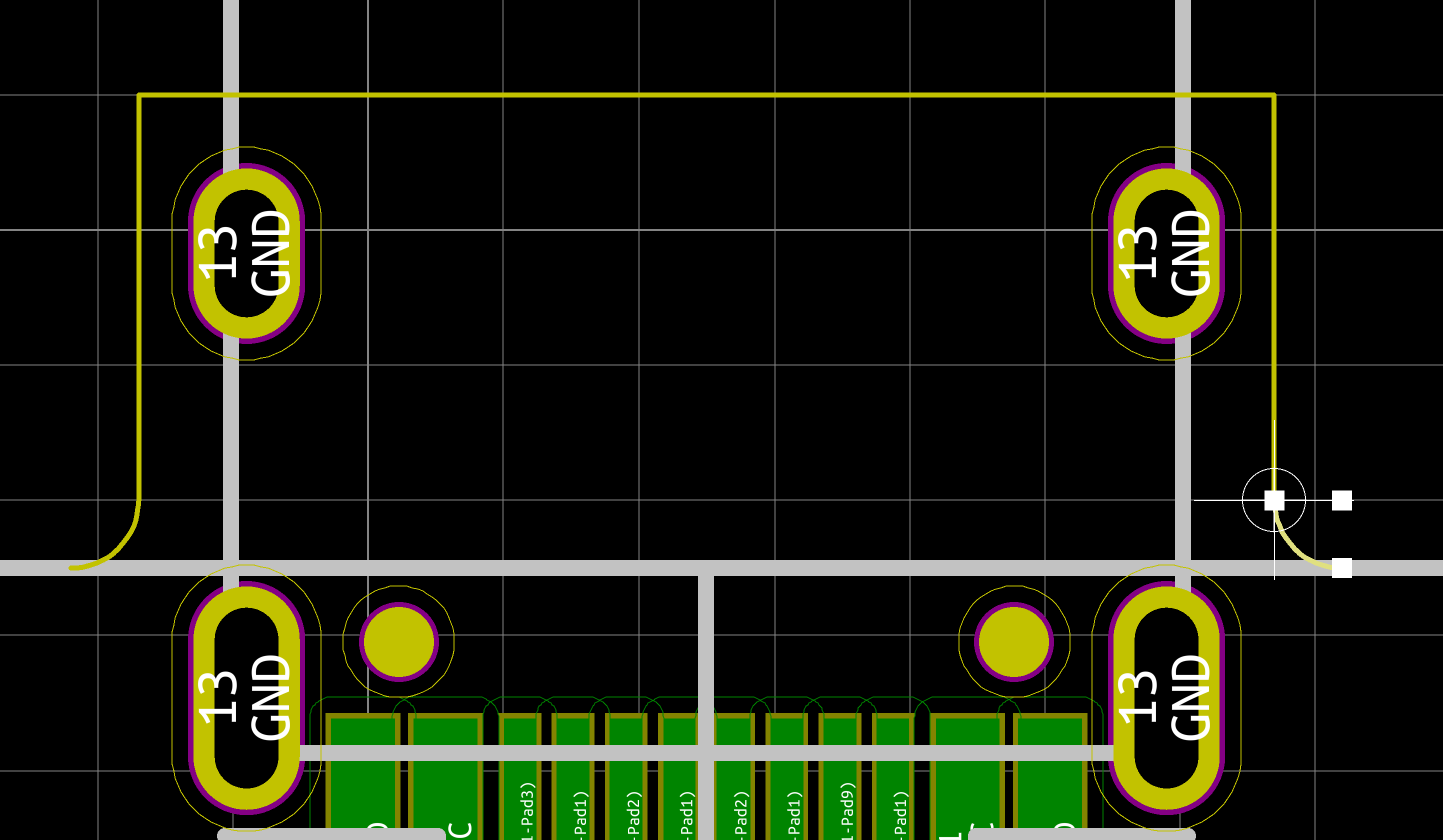
Now, inspect visually the edge cuts to make sure everything is aligned and connected. To have a better view, I recommend to hide the Dwgs.User layer (where the switches bounding boxes are drawn). I also ran the Design Rule Checker (from the Tools menu) to spot any edge cut errors:
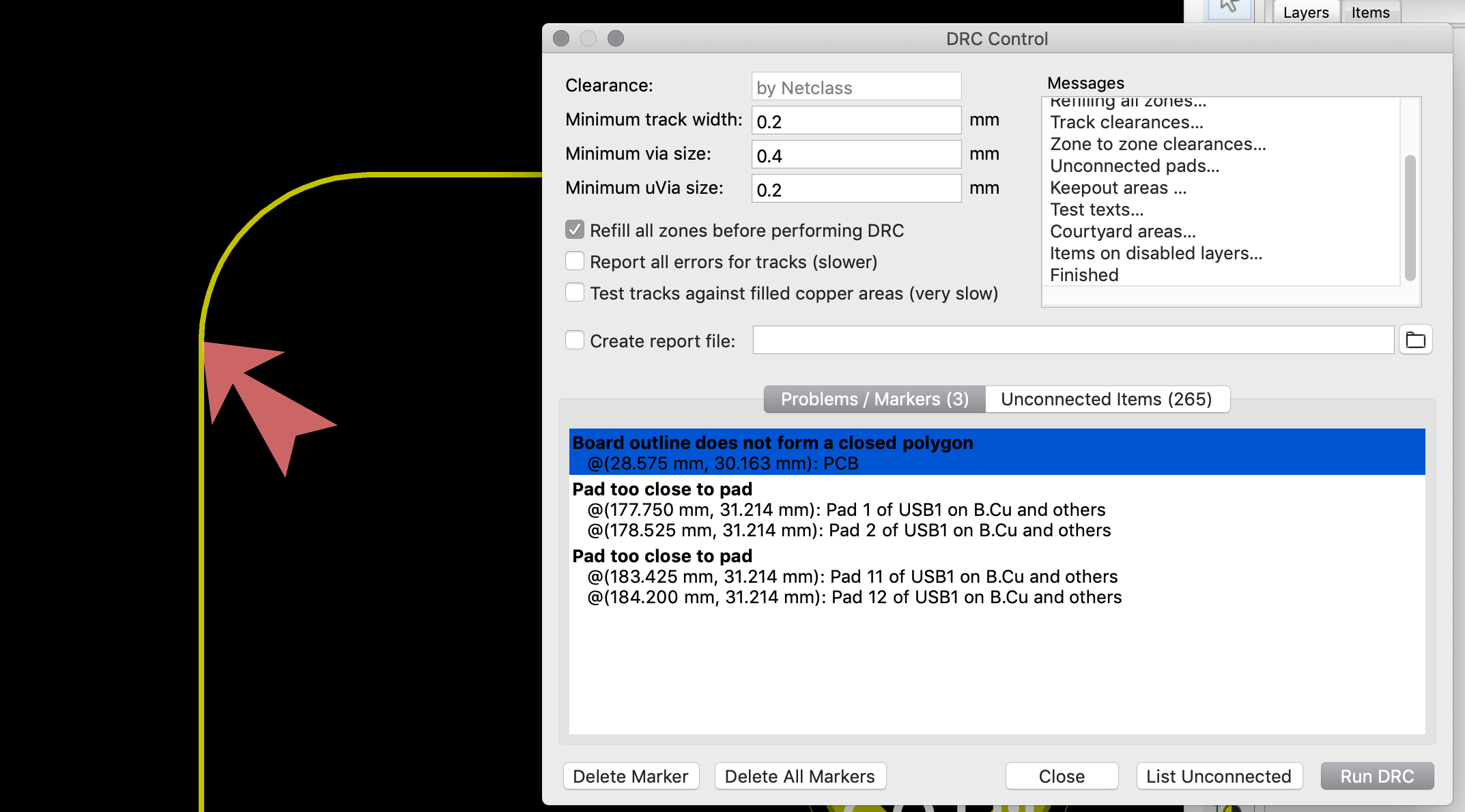
In this case the line was extending into the arc too much (by one grid step). It was easy to fix but couldn’t be found except with the DRC.
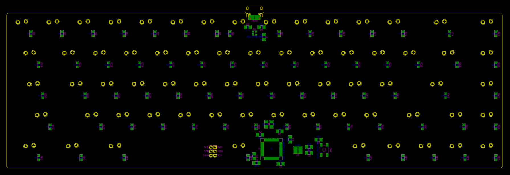
The big picture
If you followed the design so far, you should have the following PCB:
3D Visualization
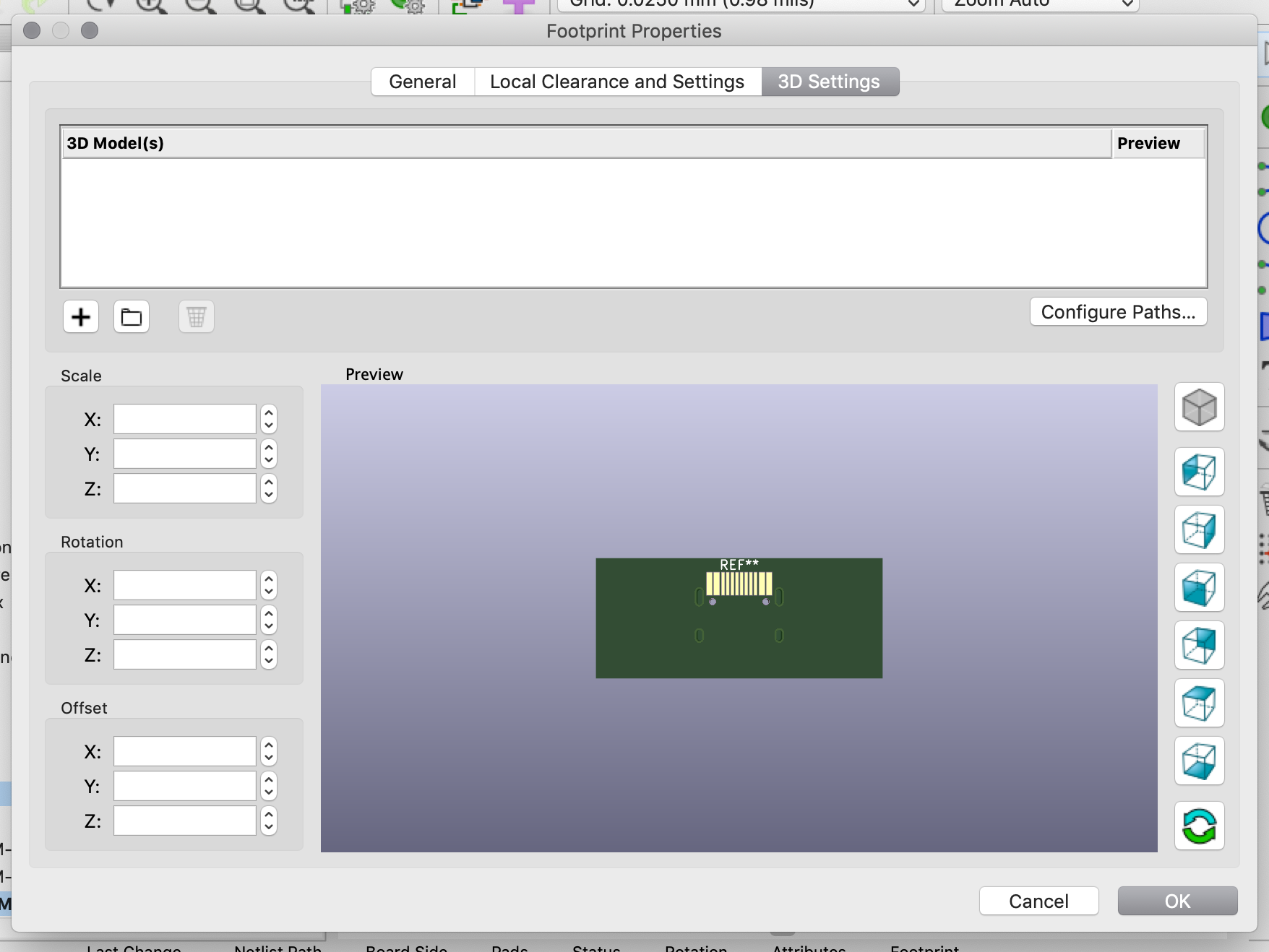
There’s a feature in the Kicad PCB editor to see the PCB in 3D. I don’t have the tracks laid out yet, but all the components have been placed so there’s something to see. Activate View → 3D Viewer to see the board top. You can rotate the board (not the best virtual ball I’ve ever used) with the mouse and see the bottom face (which contains our components). You’ll soon discover that there’s no 3D model for the USB Type-C connector. Hopefully it’s easy to add it. First edit the USB Type-C connector, then click on the Footprint Properties icon and finally click on the 3D Settings tab:
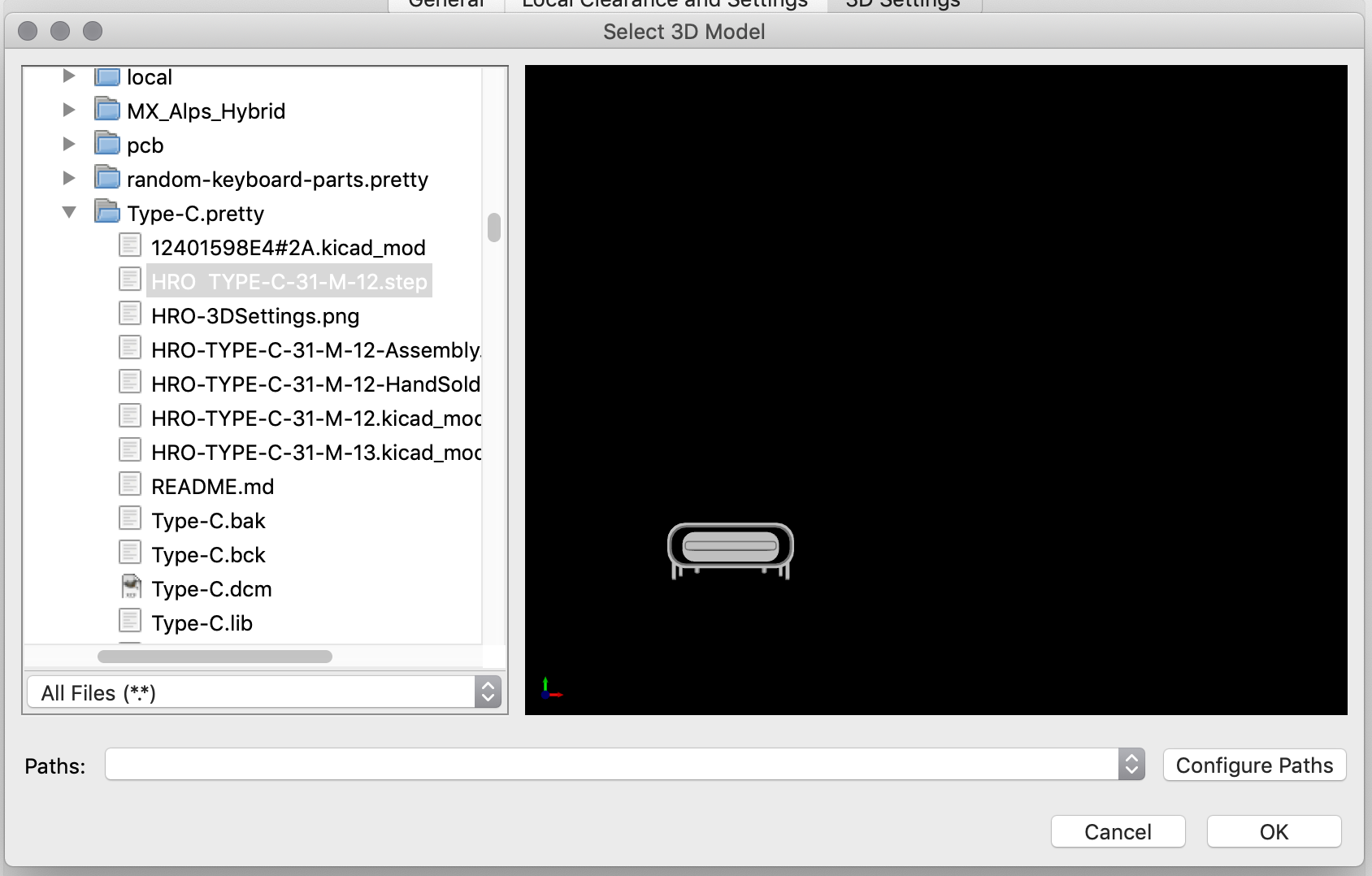
Kicad doesn’t know where to load the USB Type-C connector 3D model, click on the folder icon to add it and chose the Type-C.pretty/HRO TYPE-C-31-M-12.step file:
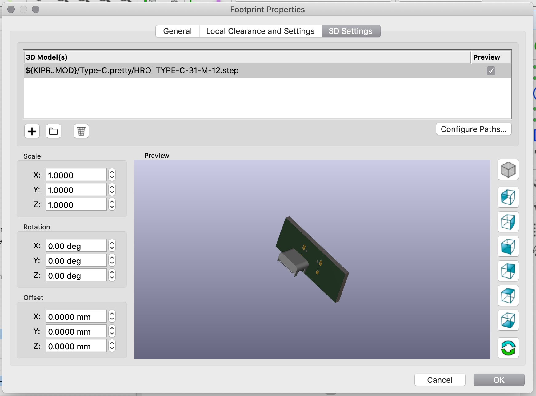
This loads the 3D model but in a completely off orientation:
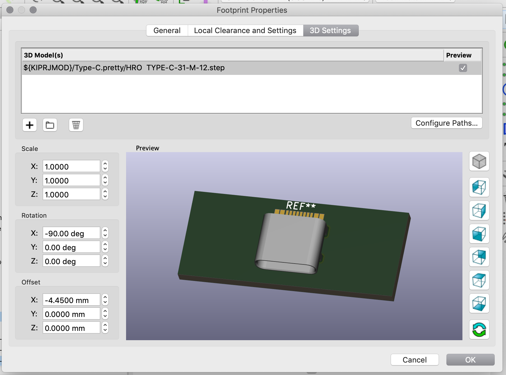
Apply the following transformation so that the connector has the correct orientation:
Save the footprint, and finally the board can be rendered with all the components:
What’s cooking next
That’s all for today. We’re still far from having a working PCB, and in the next episode I’ll cover:
- routing the traces
- power ground pour
- adding drawings on the silkscreen
- manufacturing the PCB
Thanks for following!
Want to read the next part? Then click here for the Designing a Keyboard part 3
Comments