Designing a keyboard from scratch - Part 3
Welcome for the third episode of this series of posts about designing a full fledged keyboard from scratch. The first episode focused on the electronic schema of the keyboard controller, the second one was on the components’ layout. In this one I’ll cover:
- how to route the matrix
- the MCU
- the USB datalines
- adding drawings on the soldermask
This is a long episode that took me a quite long time to produce. Feel free to leave a comment if you have any questions or find anything suspect :)
The Art of Routing
Routing is the process of connecting the various pins and pads of the circuits with copper traces while respecting the electronic schema. There are things that can and can’t be done for the PCB to be functional, for instance circuits have specific constraints for EMI, impedance matching, etc.
In the previous episode I decided to use a two layers PCB (which is the best compromise between cost and ease of routing for such projects). The switches are placed on the front layer, and because they are through-hole components they are being soldered on the back. All the rest of the components are laid out on the back of the board.
In the part 2 of this series of posts, I shown how to design the matrix schema. The matrix is a set of non-intersecting rows and columns. This means that if we were to route the matrix on the same PCB face we’d had an issue: all rows would collide with the columns.
Hopefully, since there are two layers in this PCB, I can route the columns on one side and the rows on the other side. Unfortunately there are other components to connect: the USB Type-C connector (and its ESD protection circuits), the MCU, the reset push-button, etc.
The USB Type-C connector is on the back layer at the top of the board, the MCU is also on the back layer but at the bottom. That means there are a few tracks to route vertically akin to the columns.
Inevitably some traces will intersect other traces. In such case it is possible to switch the trace to another layer by placing a via. A via is an electrical connection between two layers. The trace can then extend from one layer to another. Basically it is a hole that is metal plated to be able to conduct electricity. Note that there are different kinds of via, depending on if they cross the whole board or only some layers. In the case of two layers PCB, it will be through-hole vias.
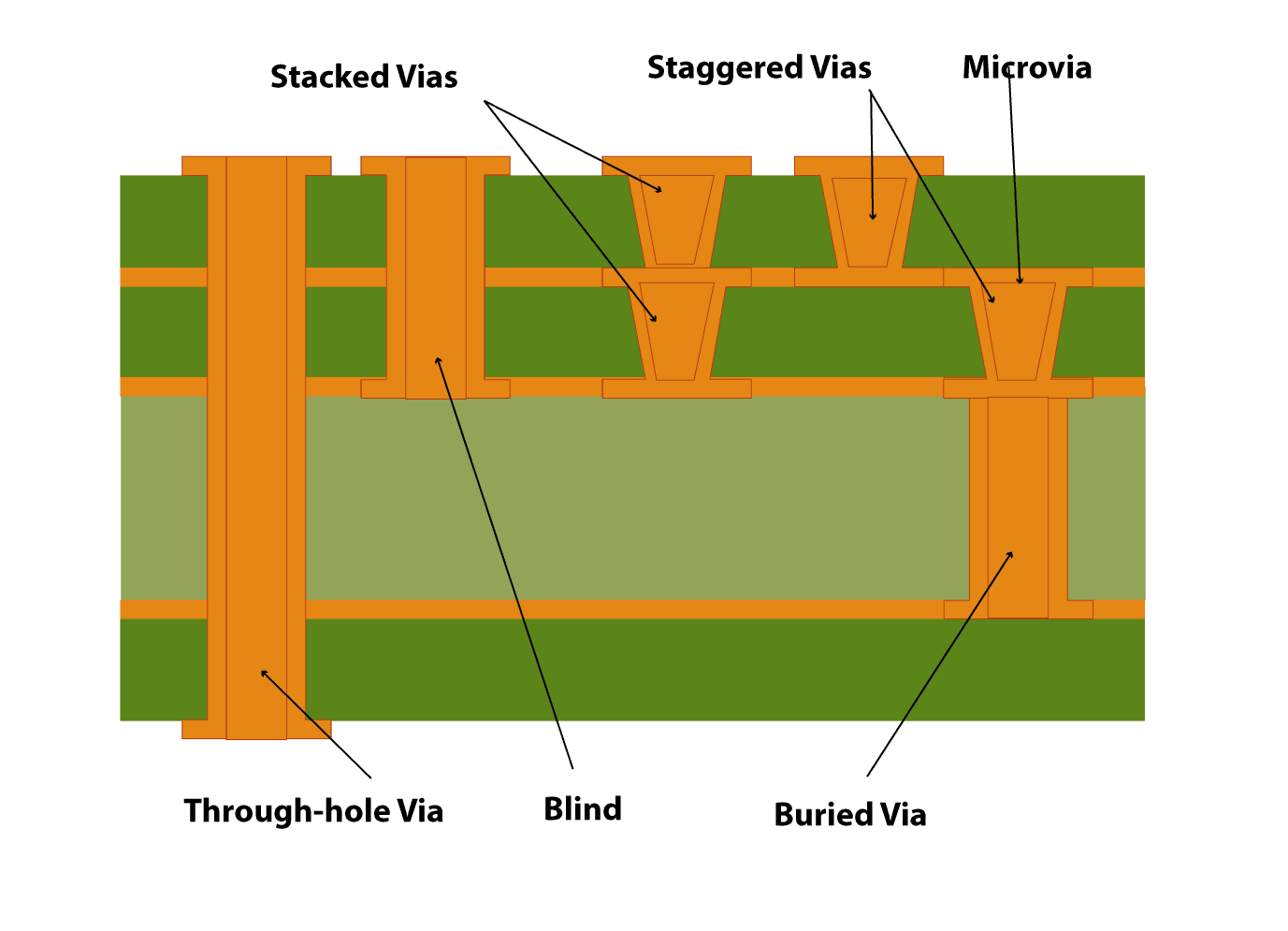
With a pair of vias in series the trace can jump to the other side and come back to its original side.
Another important thing to know is that a through hole pad (like the switch ones, but this is valid for any through-hole components) is available on both layers. This means a trace can piggy-back a switch pad to switch layer:
To prevent via abuse, the routing needs to take advantage of the number of layers. So for instance I can route the columns on the front layer, and the rows on the back layer.
But it is also possible to do the reverse:
I was forced to use vias to jump other the column col1, because the diodes are on the backside. I tried two possibilities, using vias only for the minimal jump or using vias on the pad. Notice how both seems inelegant. Putting a via on a pad is also not a good idea unless the manufacturer knows how to do plugged vias. This can be needed for some high-frequency circuits where the inductance needs to be reduced. This isn’t the case of this very low speed keyboard, so I’ll refrain doing this.
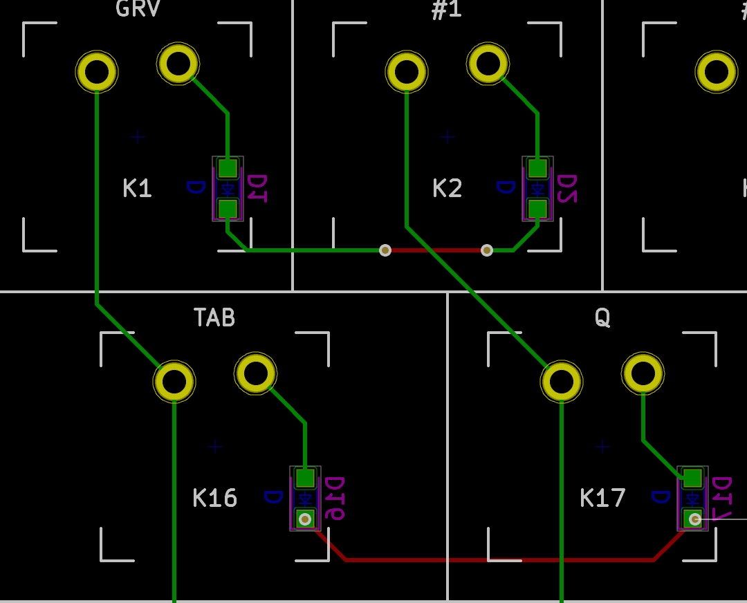
Routing matrix columns
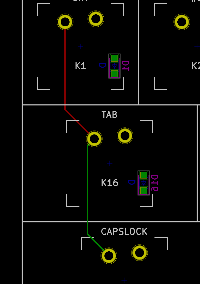
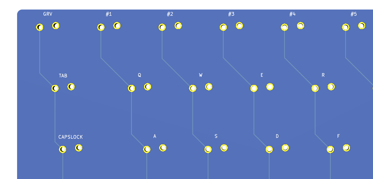
Let’s route the columns. Start from the top left switch (or any other switch), then activate trace routing by pressing the x shortcut. Make sure that the F.Cu layer is active. If it’s not the case, you can switch from one layer to another by pressing the v shortcut. Caution: if you press v while routing a track, a via will be created. To start routing, click on the GRV left pad, then move the mouse down toward the TAB switch left pad (follow the net yellow highlighted line which shows where the net is connected):
Notice that while routing a specific net, this one is highlighted in yellow, along with the pads that needs to be connected.
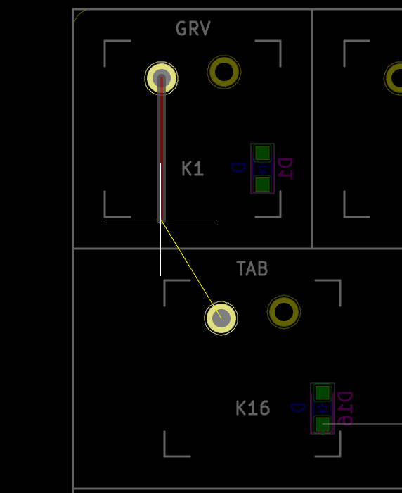
Keep going until you reach the next pad, and then click to finish the trace. Notice that the route is automatically bent and oriented properly. This is the automated routing:
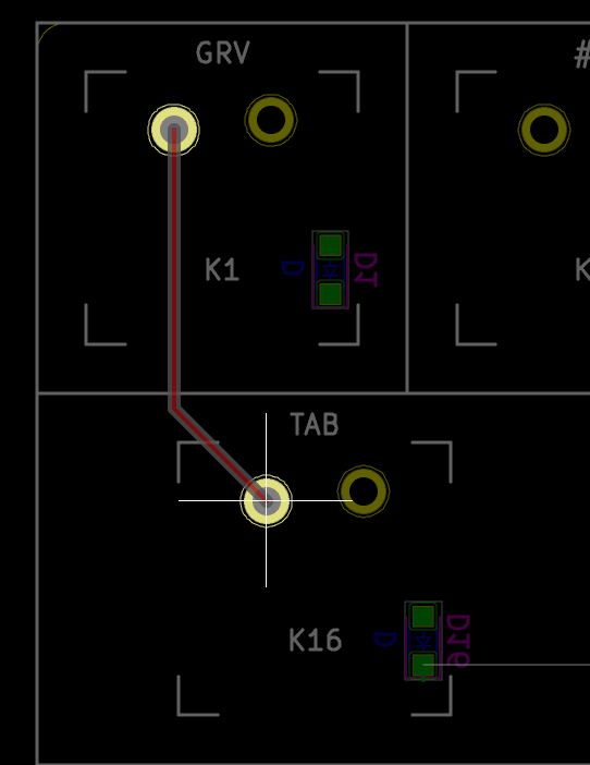
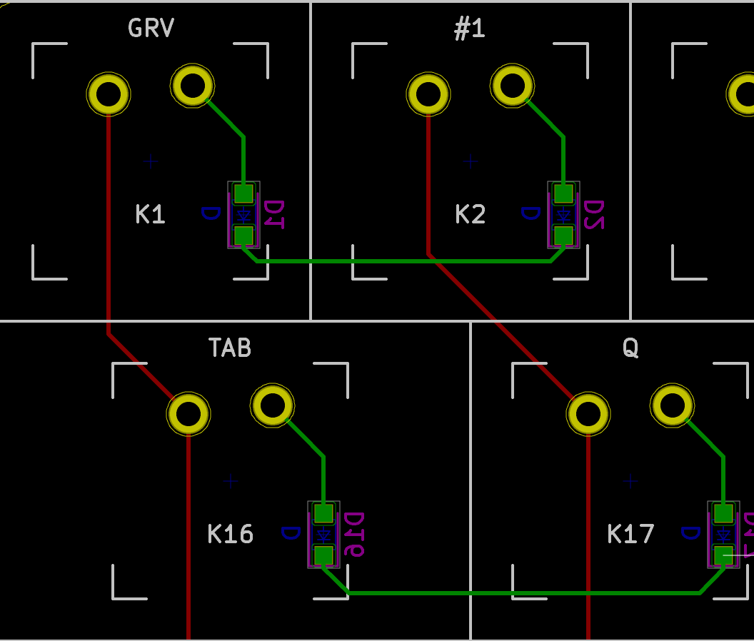
Keep going until all columns have been routed. Sometimes the trace is not ideally auto-routed by the automated routing system. In this case, it is possible to fix the problem by selecting the segment and use the Drag Track Keep Slope (shortcut d) to move the trace. For instance this trace pad connection could be made better :
Dragging the track with d until I eliminated the small horizontal trace:
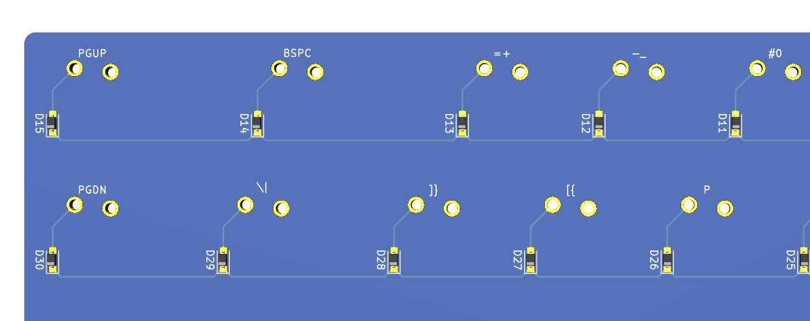
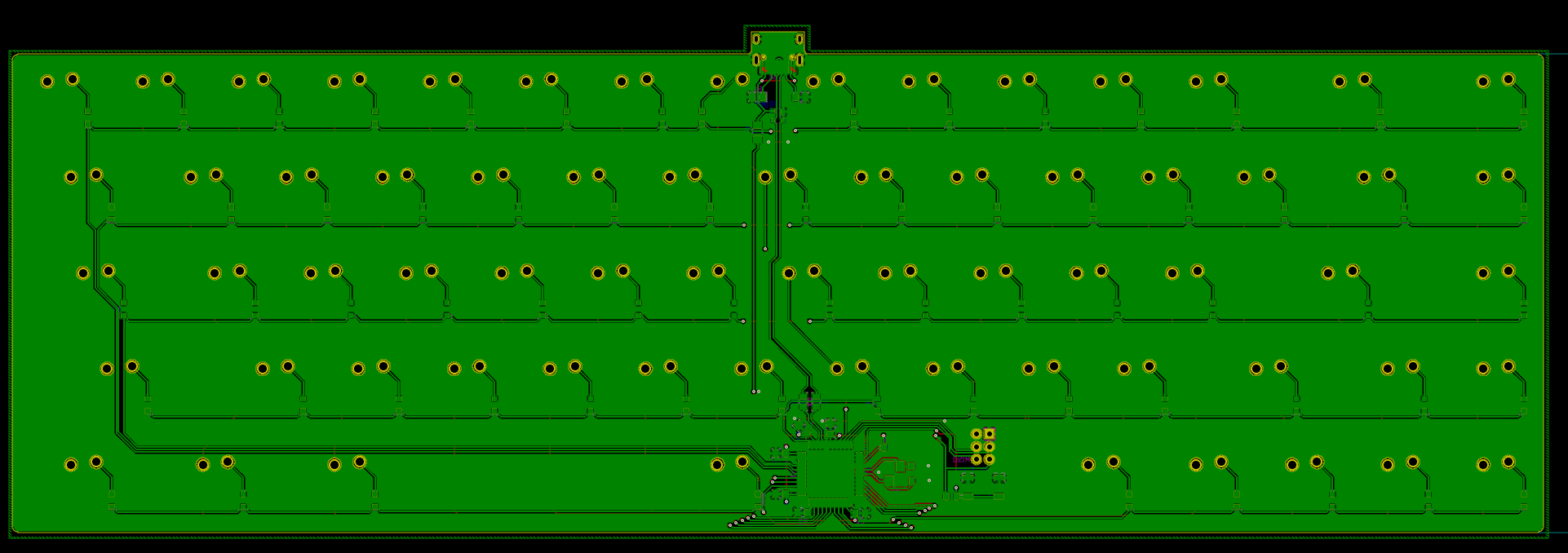
When all the columns are completed, the PCB looks like this:
Notice that I haven’t connected the columns to the MCU yet, hence all the nets are directly linked to their assigned pads with those white lines.
Using the Show local ratsnest function we can highlight the columns nets, and verify that the connection scheme in part 2 is correct.
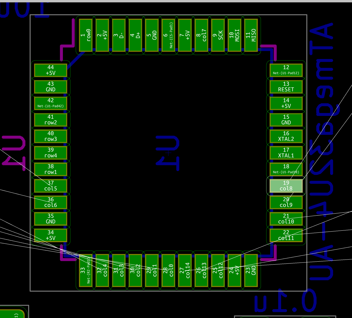
The idea was to have the columns on the extreme left or right be assigned the bottom part of the MCU (respectively left and right pads), and the center left columns (col5, col6) the left pads, the center columns col7 a free top pad, and the center right columns col8, col9 the right pads.
This gives this result:
But before connecting the columns to the MCU, it’s better to route the USB data-lines and power rails.
USB differential pair
The D+/D- USB data lines form what is called a differential pair. The idea is to send a complement signal on two wires instead of the normal signal on one. Traditionally a component uses GND as the reference for a signal in a single wire. This can be subject to EMI and noise. In a differential pair (and provided the impedance matches on both wire), the noise will affect both wire the same way. Since the MCU computes the difference between the two signals to recover the correct value, the noise is removed (because it is the same on both lines). The differential pair is thus much more immune to EMI and noise than a single trace.
Thus, differential pairs needs to be routed with care. Both trace needs to obey some important rules listed below.
Respect symmetry
To conserve coupling it’s best for the differential pair traces to keep their symmetry as good as possible.
Match Trace Length
The noise-cancelling advantage of a differential pair works only if both signals arrive at the same time at the endpoint. If the traces have different lengths, one of the signal will arrive a bit later than the other, negating the effect. There’s a tolerance though, especially since this keyboard USB differential pair will run at the USB Full Speed standard (12 Mbit/s).
It’s possible to compute the time difference of the signals in function of the length difference. With the Full Speed standard a few centimeters difference will not incur a difference in arrival time, but this wouldn’t be true with high-speed signals. It’s best to keep the good practice of matching length all the time.
There’s no function in Kicad to check trace length, hopefully the trace length plugin can be used to check both traces length of the pair.
Reduce distance between traces
Obviously this will take less space on the PCB, which is good. But also the differential pair return current will flow in the ground plane below (if there’s one), possibly creating a current loop generating noise, if both tracks are not coupled enough because of their relative distance. This is again less an issue with USB Full Speed signals like the one this keyboard deals with (or with 2 layers boards without ground planes).
Minimize number of vias
Each via adds inductance to the trace. It is usually recommended to not route those differential pairs through vias. But if vias have to be used anyway, make sure to use the same number of vias for both traces of the pair. With USB Full Speed signals, adding a few amounts of vias would probably not be detrimental, but it’s better to keep those traces on the same layer as much as we can as a good habit. Make sure to place all the IC so that there’s no need for differential pairs to change layers. That’s also the reason differential pairs should be routed first.
Spacing around differential pairs
The differential pair should not be too close to other signals or other differential pairs. A good rule of thumb is to apply a spacing of 5 times the trace width (this is known as the 5W rule).
Where the differential pair comes close to high speed signals (for instance clock traces), the spacing must be increased again (for instance 50mils). Differential pairs should also be spaced from other differential pairs to prevent cross-talk (use the same 5W rule).
Watch the Return Current
Spoiler alert: all circuits form a closed loop. The signal in a differential pair is a current that needs to flow back to it’s source at some point. At higher frequencies, the return current will follow the lowest impedance path. This usually happens to be the closest reference plane (a ground or power plane if there’s one). If there’s a void or a split in the reference plane, the return current will have a longer path leading to excess electromagnetic emissions, delayed signal, etc.
Don’t route close to crystals
The differential pairs should not be routed under or near a crystal oscillator or resonator.
Crossing a differential pair
When a single track or another differential pair crosses (on a different layer) a differential pair, do it with an angle of > 30º and < 150º to minimize cross talk. To make it more easy target 90º intersections.
Do not use striplines
A stripline is a layer trace embedded in a dielectric medium itself sandwiched by two copper plane. On the reverse a microstrip is a trace at the surface (not embedded). It’s best to route differential pairs as microstrips.
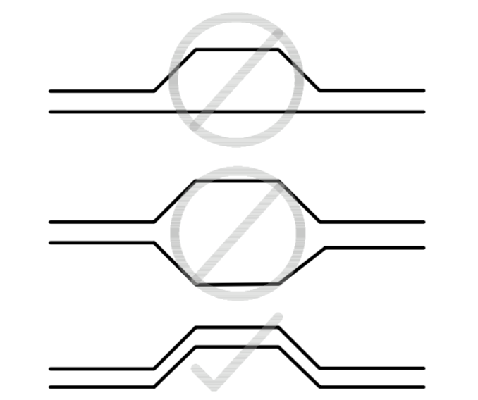
Avoid Bends
If possible, the differential pair should never do a straight U-turn. When bending, maintain a 135º angle all the time.
Keep away from edges
The recommendation is to keep at least 90mils between the traces and the ground plane edges.
Control the trace impedance
The USB 2.0 standard requires the transmission lines (ie cables and connected PCB tracks) to have a differential impedance of 90 ohms (which translate to a single line impedance of 45 ohms) +- 10%.
Maintaining the impedance is capital to prevent high frequency signals to bounce. To perform controlled impedance routing, you need to compute the single trace width and spacing (there are calculators online and even one in Kicad; the free Saturn PCB calculator is a good reference but works on Windows only).
It’s relatively easy to control the impedance if there’s a continuous ground plane not far below the tracks (so it’s best to route those on 4+ layers PCB). But for a 2-layers PCB, assuming one of the layer is an uninterrupted ground plane, the trace size would have to be 38 mils spaced with 8 mils to match the 90 ohms impedance. This is because the height of the dielectric board is around 1.6 mm for a 2 layers board, whereas it is less than a 1 mm between two copper layers on the same side of the board.
Hopefully, if our traces are shorter than the signal wavelength there’s no need to implement controlled impedance. With a tool like the Saturn PCB Calculator we can estimate the USB Full Speed wavelength and thus our max trace length.
The USB Full Speed rise time is between 4 ns to 20 ns. When injecting the worst case of 4 ns in the Bandwidth & Max Conductor Length calculator, the result is a bit more than 18 cm. Since this keyboard is currently 9.5 cm wide and the USB D+/D- will be traced as straight as possible, the differential pair length will be well within the safety margin. Based on this, I’m going to use 10 mils as trace width and spacing.
Forbid stubs
Stubs should be avoided as they may cause signal reflections. For USB, this is seldom a problem as the data traces are point-to-point.
Want to know more?
Most of these recommendations were gleaned from TI High-SpeedLayoutGuidelines, Silicon Labs USB Hardware Design Guide, Atmel AVR1017: XMEGA - USB Hardware Design Recommendations, Intel EMI Design Guidelines for USB Components. I also recommend reading Eric Bogatin - Signal and Power Integrity - Simplified and Henry W. Ott - Electromagnetic Compatibility Engineering. Refer to those documentations for more information.
Routing
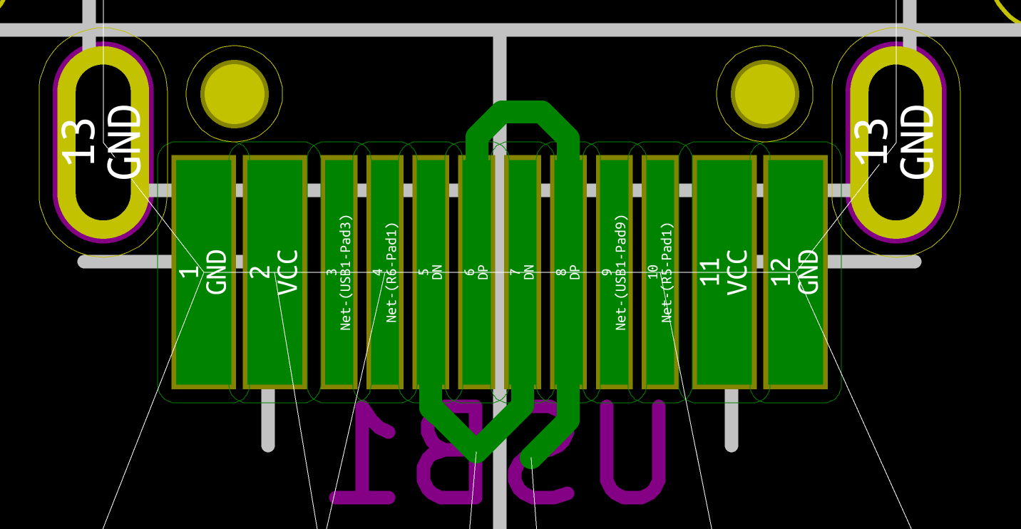
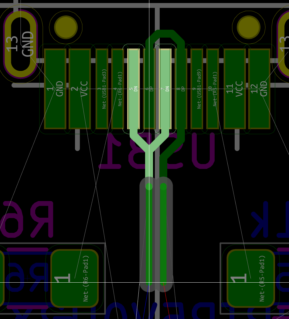
Now let’s apply this knowledge to this keyboard. First I need to prepare the USB connector data lines: since there are 4 pads for the two datalines (to support reversibility) they need to be connected together:
Use the Route → Differential Pairs feature and start laying out the traces from the connector. Uh oh, an error pops-up:
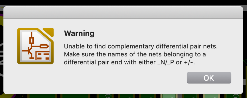
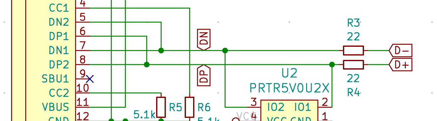
To be able to route a differential pair, Kicad requires its nets to obey a specific naming. Net names should end up in P/N or +/-, which is not the case here. The USB pads nets have no name, as they acquire their name only after the impedance matching resistors. To correct this, I just need to assign name to the wires in the schema editor:
And finally using Update PCB from schematics, I can start routing the USB data-lines (using the Route → Differential pair function):
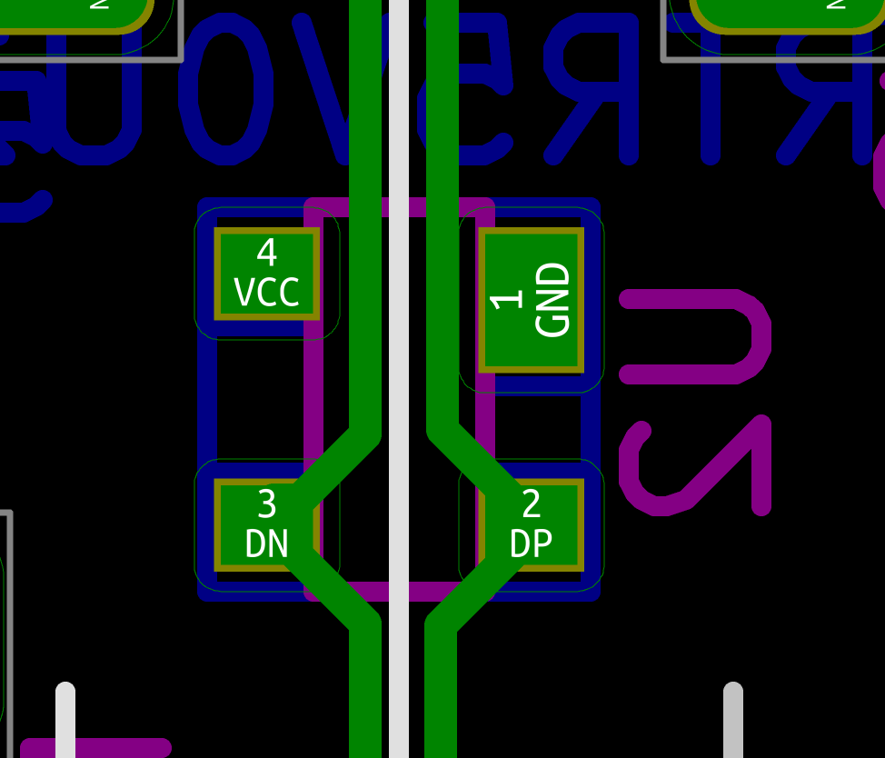
The next step is to connect the differential pair to the PRTR5V0U2X. Unfortunately Kicad is not very smart when connecting a differential pair to pads. It’s better to stop drawing the differential pair, switch to single track routing mode and connect the pads to the differential pairs. Since it’s important to minimize stubs, it’s best to uncouple a bit the differential pair to connect it to pads, like this:
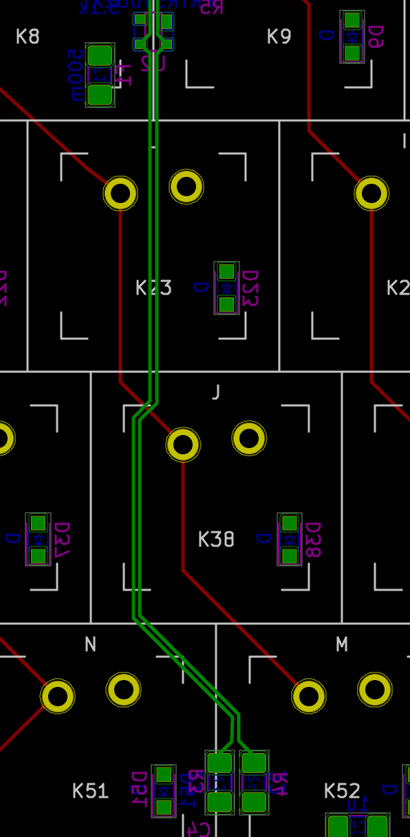
Then, the differential pair can be routed to the pair of impedance matching resistors (which are located close to the MCU):
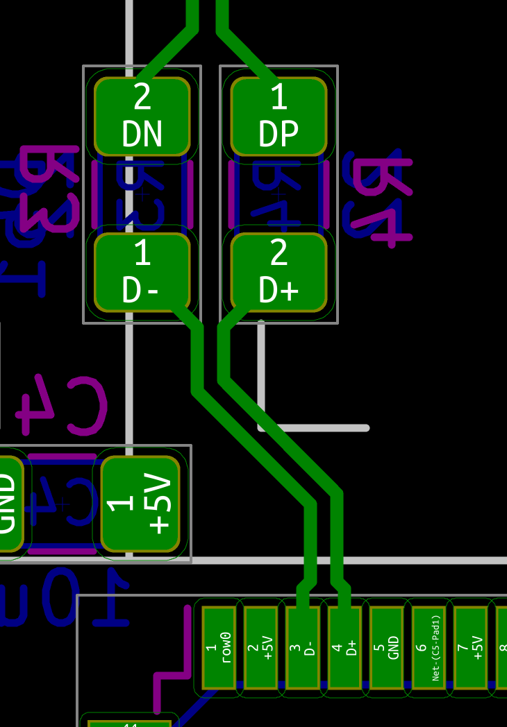
To connect the resistors to the MCU with a differential pair, it’s easier to start from the MCU by using the Route → Differential Pair function and connect the MCU pads to the resistors pads:
Now, I can check both trace lengths with the Measure Length of Selected Tracks plugins. To do that, select one trace of the pair, and use the u shortcut to select it fully. In the case of this keyboard, I got 70.05 mm for the left traces and 69.90 mm for the right one. This is small enough to not try to optimize it.
The final routing of this differential pair looks like this:
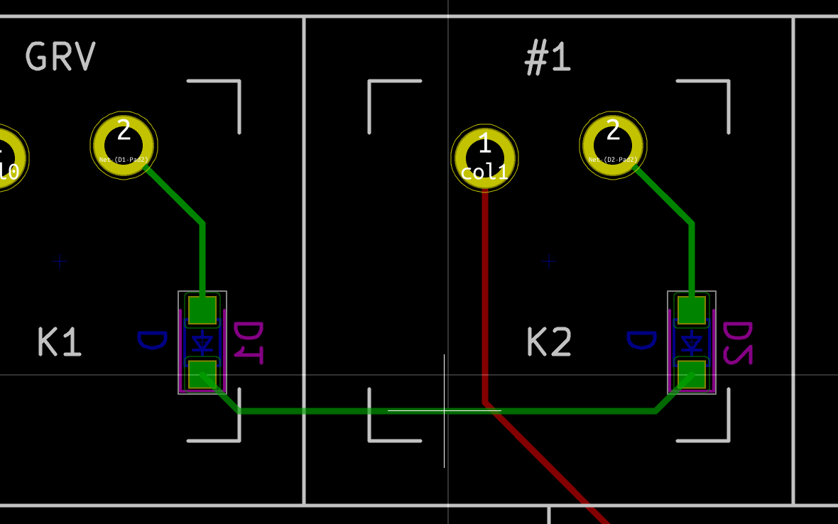
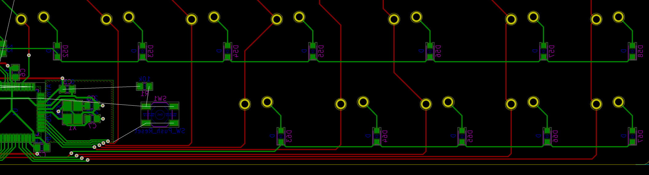
Routing switch rows
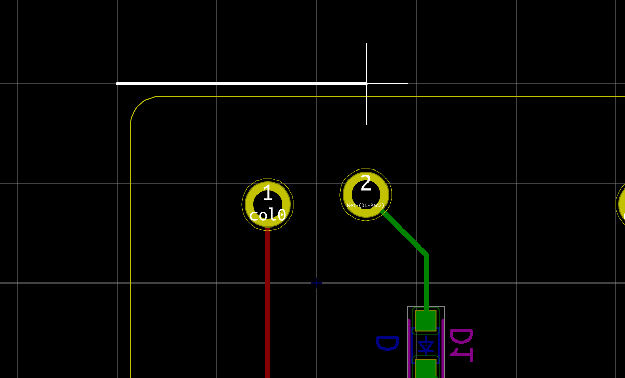
The first step is to connect the right switch pad (#2) to its diode anode for every switch:
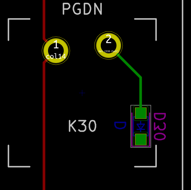
Then connect all cathodes together with a track forming the row. Draw a straight line first:
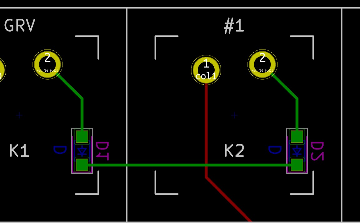
Then use the d shortcut to produce a more appealing form by dragging the track toward the bottom:
Do that for all the switches, but do not connect the rows to the MCU, nor cross the USB differential pair yet, because there will be some choices to be made and experimentation.
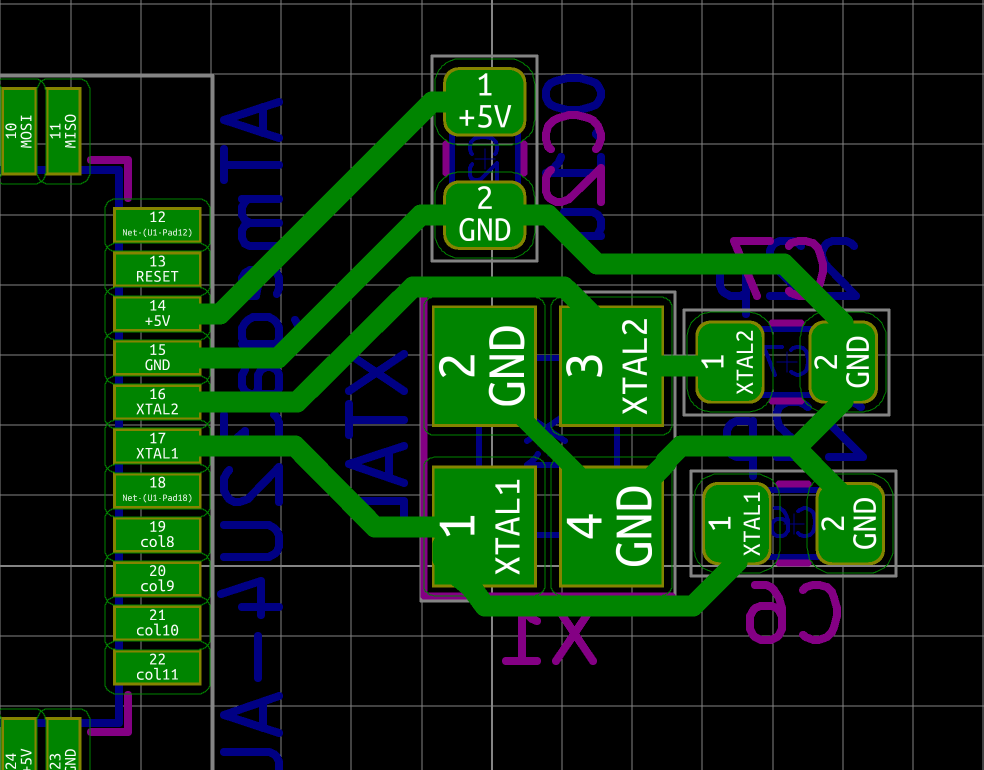
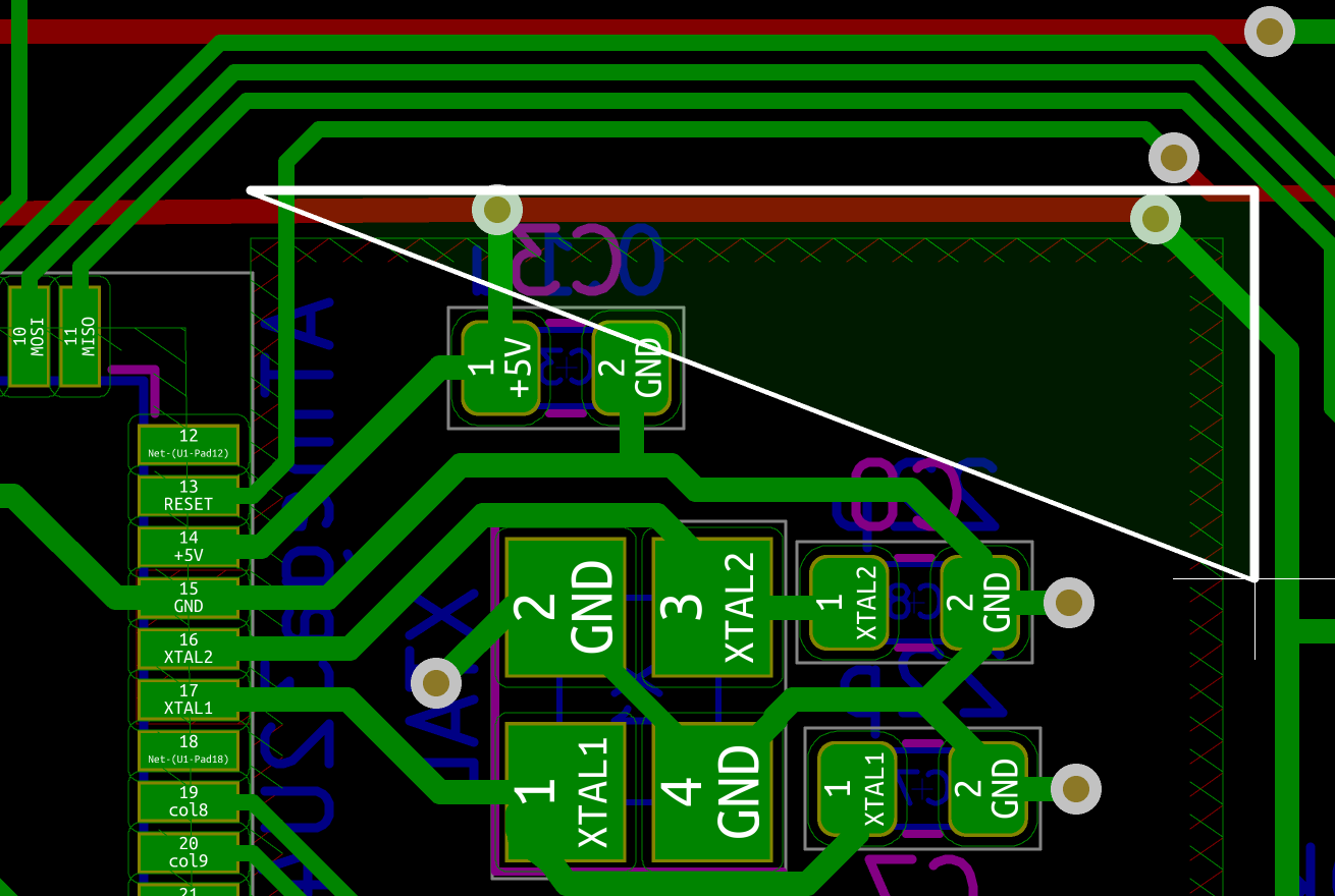
Routing the crystal oscillator
Routing the crystal oscillator is easy as there are few tracks and components. The crystal generates a square wave signal at 16 MHz. A square signal is the combination of a lot of powerful harmonics in the frequency domain. Those are an issue for EMC, so special care has to be applied for placement and routing of the clock circuits.
The first rule is that we have to make the XTAL1 and XTAL2 trace as short as possible. This means the crystal has to be as close as possible to the MCU, this is in order to minimize parasitic capacitance and interferences. For the same reason, avoid using vias in the crystal traces.
The second rule is that we have to space other signals as much as possible to prevent the clock noise to be coupled to other traces (but also the reverse). To prevent as much as possible this effect, it is recommended to add a GND guard ring around the crystal traces.
The main problem with crystal oscillators is the return current. Every electrical circuit form a loop, so the current that gets in the crystal, needs to go back to somewhere for the crystal oscillator to work. This return current is also a square signal containing high frequency harmonics. The problem is that the loop formed to return the current is a kind of antenna. If it is large, it will radiate a lot of EMI which we want to minimize (and also if it’s an antenna it will be susceptible to external emission which we also want to minimize). I’ve seen design with a general ground and vias connected to the crystal GND: in such case this pour becomes a nice patch antenna. If we were to design this keyboard with a ground pour, the one under the crystal oscillator should be an island not connected to the rest of the ground pour to prevent radiating everywhere and to make sure the current return loop is as small as possible. In fact, it’s even better to add a ground pour guard ring on the same layer as the crystal (the loop formed in this case will be shorter than crossing the 1.6 mm PCB dielectric).
The 22pF load capacitors should be placed as close to the crystal as possible.
Let’s start by connecting the crystal oscillator to the MCU (both XTAL1, XTAL2 and GND):
Then using the Add Filled Zone tool (select the GND net), we’re going to draw a rectangle around the crystal:
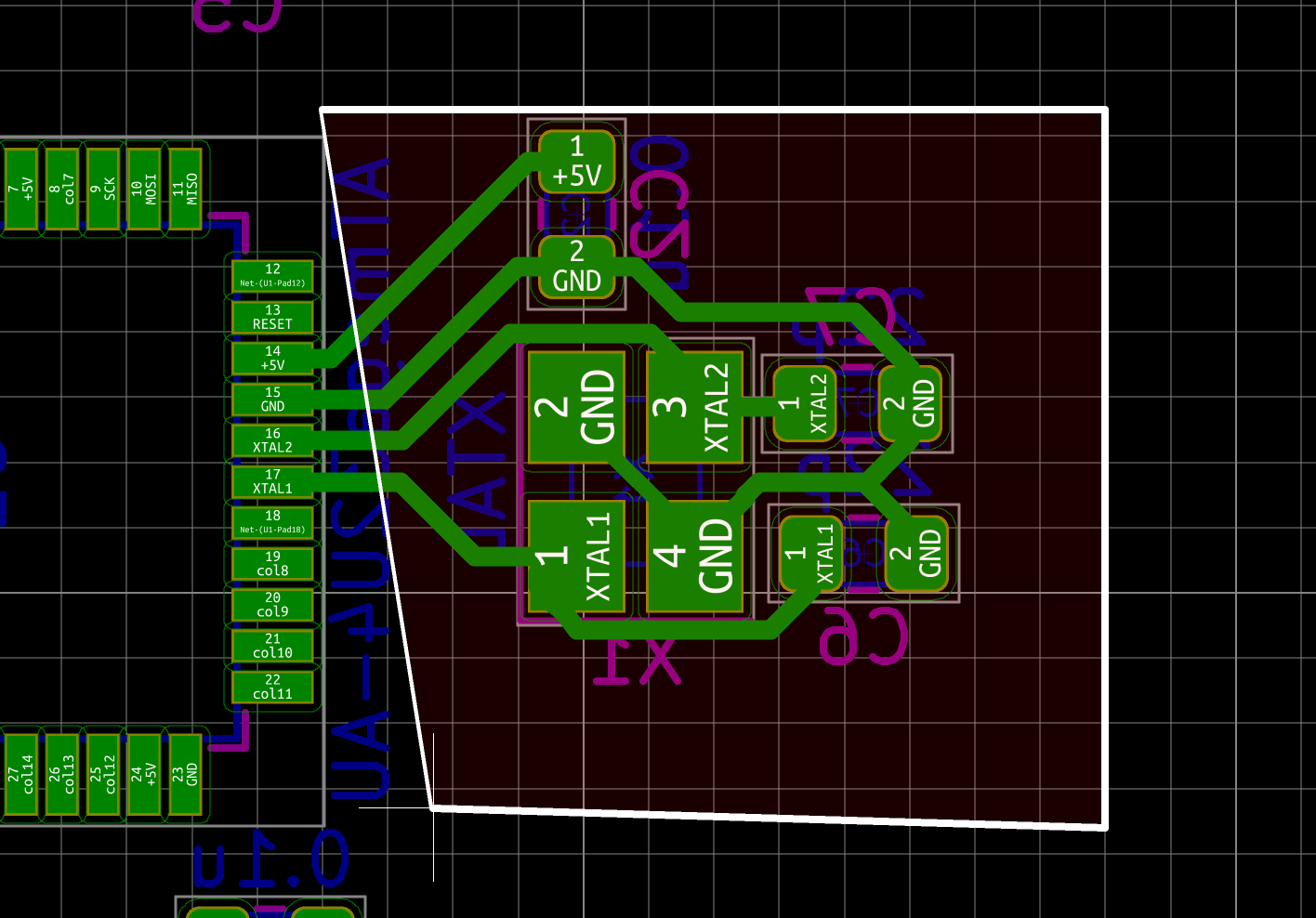
If we want to add a copper ground island in the other layer (F.Cu), we can do this easily by right clicking one of the control point of the filled zone we just added and use Zones → Duplicated Zones onto layer, then select F.Cu. This zone will not be connected to anything, so we have to add a few vias:
This isn’t complete, we should probably extend the underlying zone under the XTAL1 and XTAL2 MCU zone. First select the F.Cu layer, then right-click on the Create Corner function to add a control point. Do it again and extend the zone under the GND, XTAL1 and XTAL2 pads:

Routing the power rails
The next thing to do is to power the active components. It’s always best to route power and ground traces before the signal traces. Our signal traces can be moved around, they are not critical and are narrower than power traces.
Hopefully there’s only one active component in this keyboard the MCU (keyboards with leds, underglow rgb, rotary encoder might have more than one active component). The power comes from the USB port delivered directly by the host.
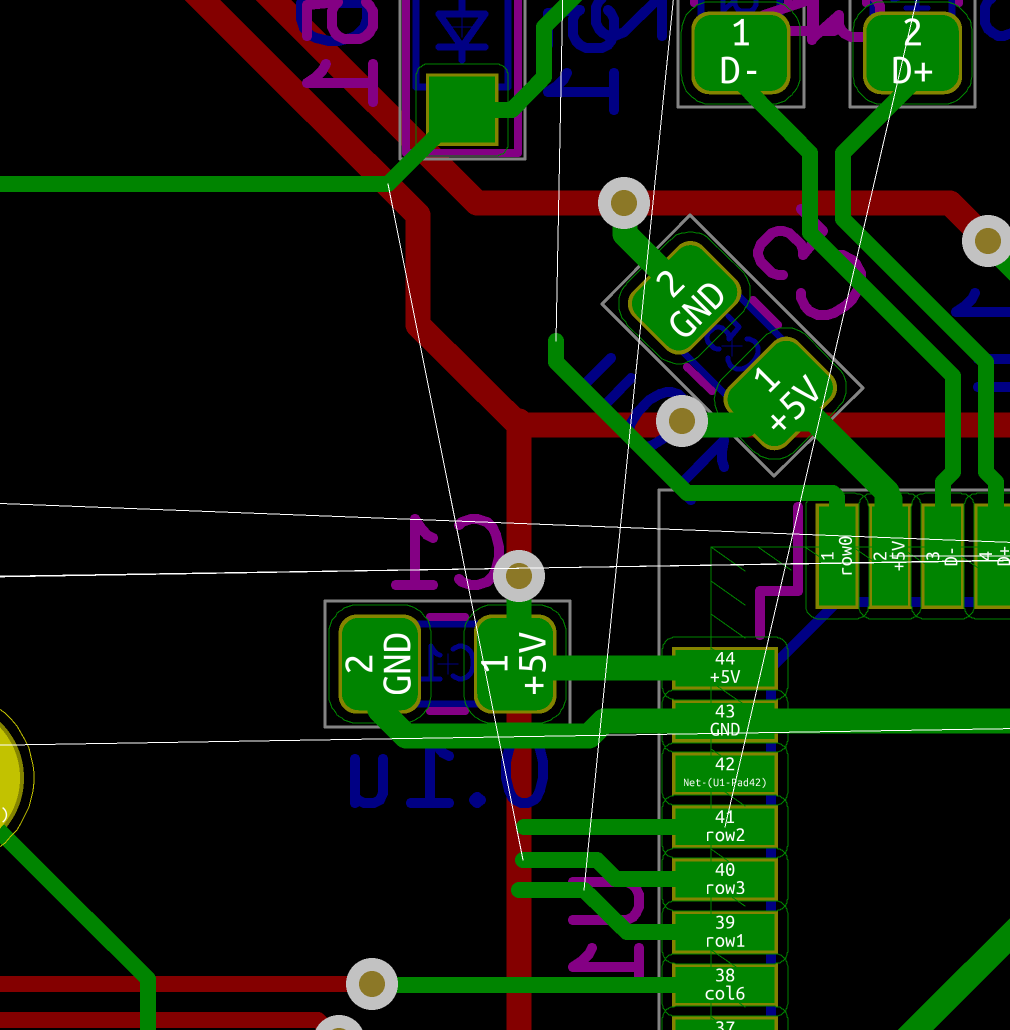
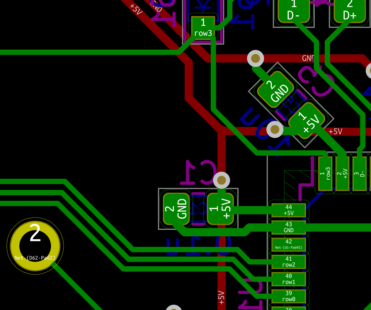
The first step is to wire the USB Type-C power traces (and also the CC1 and CC2). There are several possibilities, depending on where we want the +5V and GND to come from (since there are 2 pads with those nets on the USB connector to support both orientations).
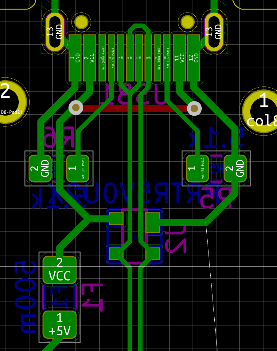
Notice that I haven’t yet wired GND. Then I can route +5V down to the MCU. I deliberately spaced the trace from the D+/D- USB differential pair to prevent it to couple into the power trace (remember the 5W rule from earlier?)
This power trace needs to deliver power to all the VCC pads of the MCU. The best way to do that is to use a grid system around the MCU on the other layer. Do not close the loop, that would be quite bad.
At the same time I connected the GND pads together with a kind of badly shaped star. I’ll replace it with a local ground pour, but if not, the star would have to be redesigned to have less acute angles. There’s an interest in having a ground pour behind the MCU (on the same layer), it will help conduct the generated heat and serve as a poor’s man radiator.
Even though I’ll use a ground pour on the front and back layer, it’s better to materialize the GND trace to the MCU. If possible I’ll come back and simplify the routing when those pour will be laid out. Meanwhile, the PCB would still be functional:
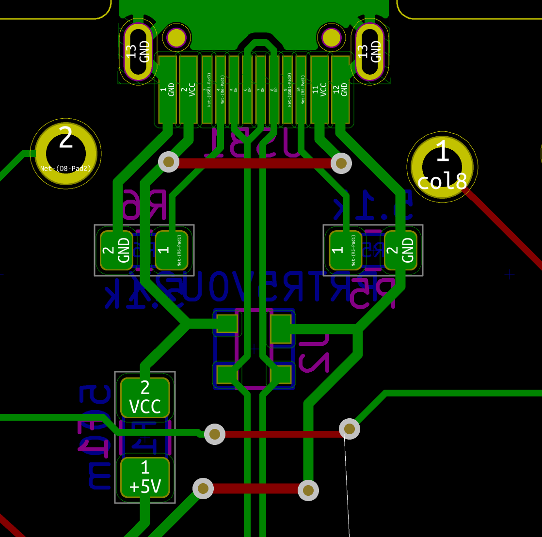
Then route the GND trace close to the +5V one down to the MCU:
Make sure to not create any GND loops.
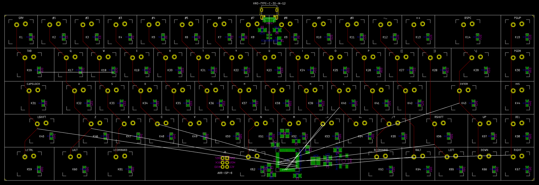
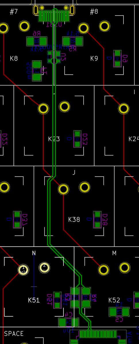
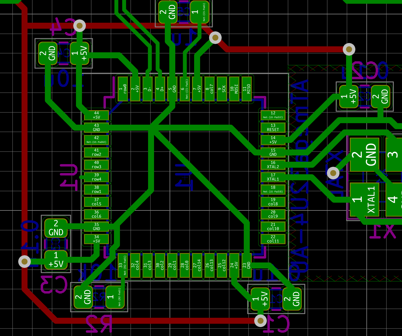
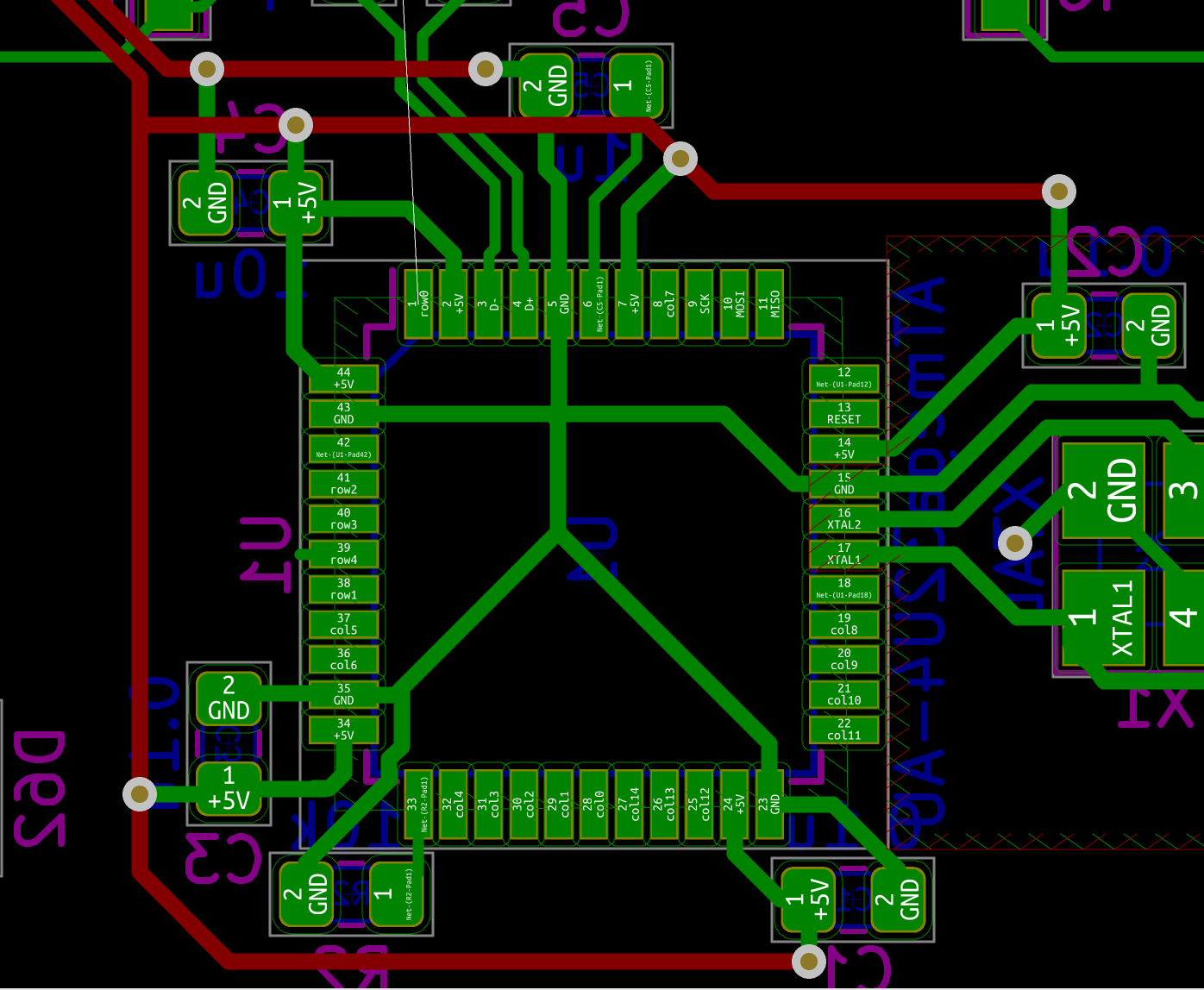
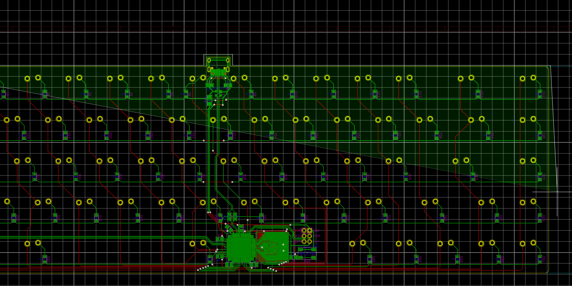
Connect the matrix
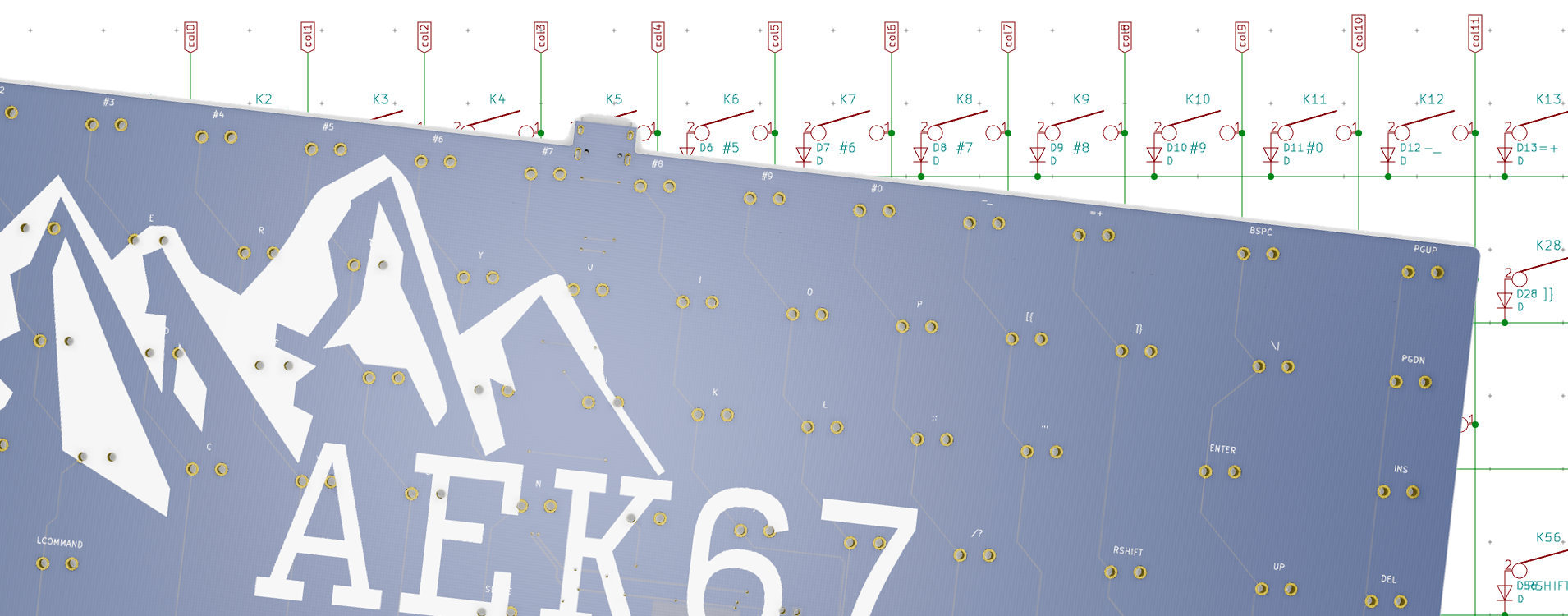
I’m going to connect the matrix. This will also allow checking if the projected connection scheme on the MCU will work or not.
I’m used to starting from the MCU and progress toward the matrix rows and columns. A good way to do that, is to start some kind of bus from the MCU pads going globally in the direction of the rows or columns to connect like this:
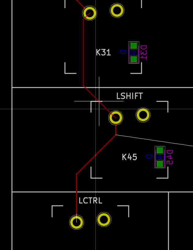
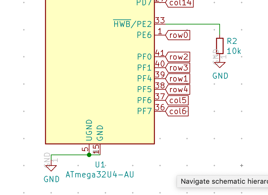
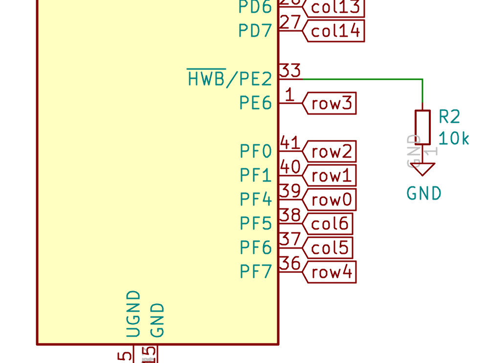
While doing that, it appears that there is a small issue on the left part of the MCU. row4 has been placed right between row1 and row3:
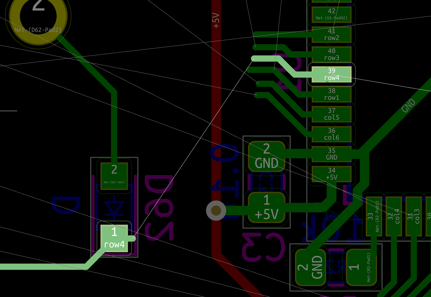
Ideally, row4 should be on the MCU pad 38 because it is to be connected directly at the bottom, while row1 and the other rows have to be connected on the left or middle part of the PCB.
Going back to the schema, it is easy to swap row4 and row1:
Routing again a bit more the left rows and columns, and it looks like it’s not yet perfect. There’s a conflict between col5, col6 and row4:
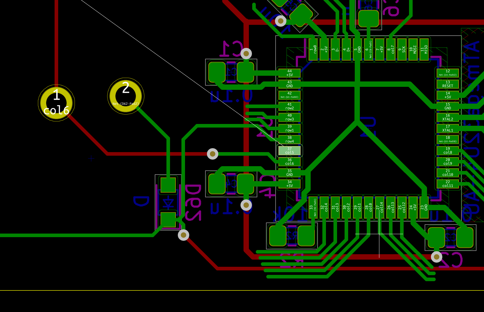
It seems much more natural to have row4 at the bottom on pad 36, then col5 and col6 (from the bottom to up), this prevents crossing those three tracks:
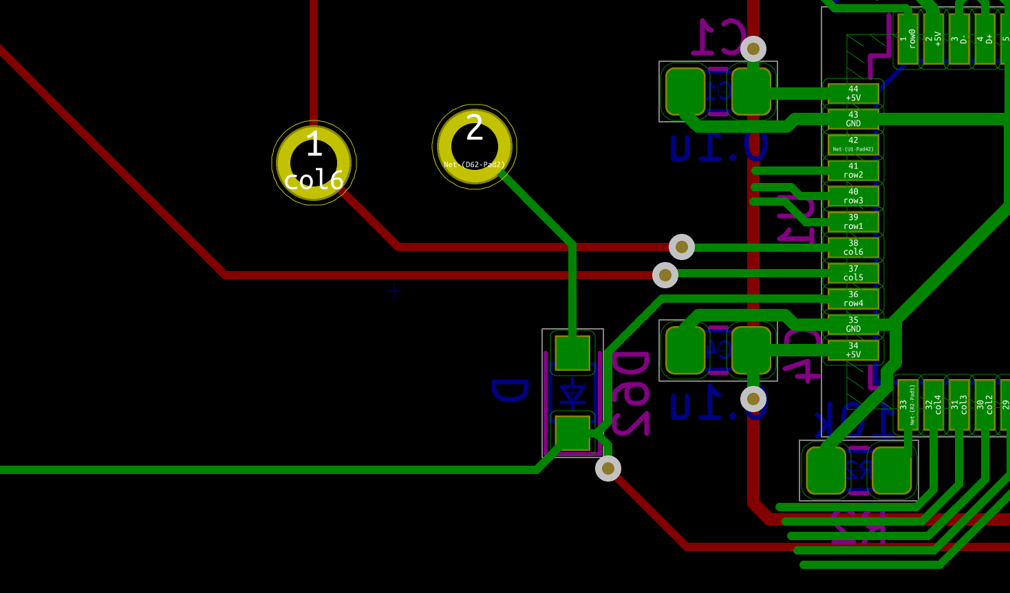
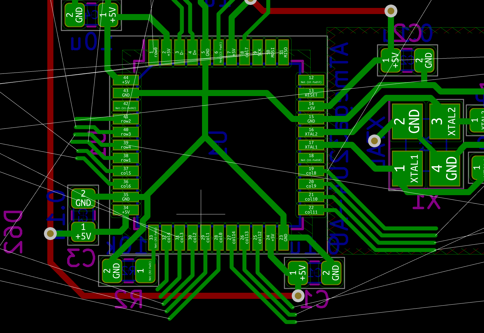
To connect the left columns (from col1 to col5), the more appealing way to do that is to group the traces as a kind of bus that connects to a pad on the last column row. Since the columns are connected on the F.Cu layer, it makes sense to convert the B.Cu traces out of the MCU with vias:
If all the traces follows the same model, it can be made visually appealing:
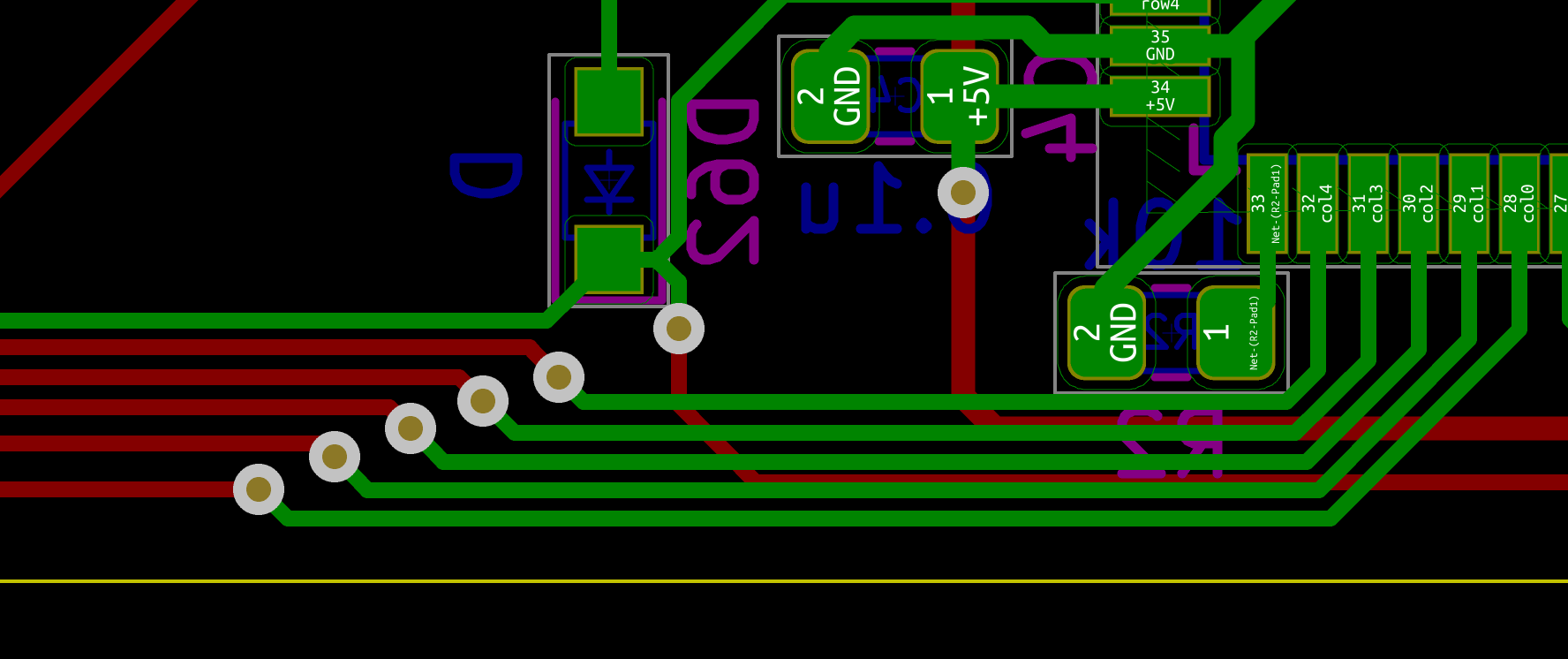
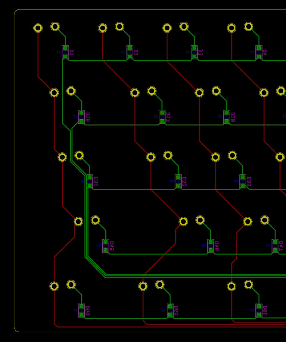
Now let’s hook the right columns (col8 to col14). Once again the idea is to group the traces together, first on B.Cu then switch to F.Cu to be able to cross the B.Cu row4:
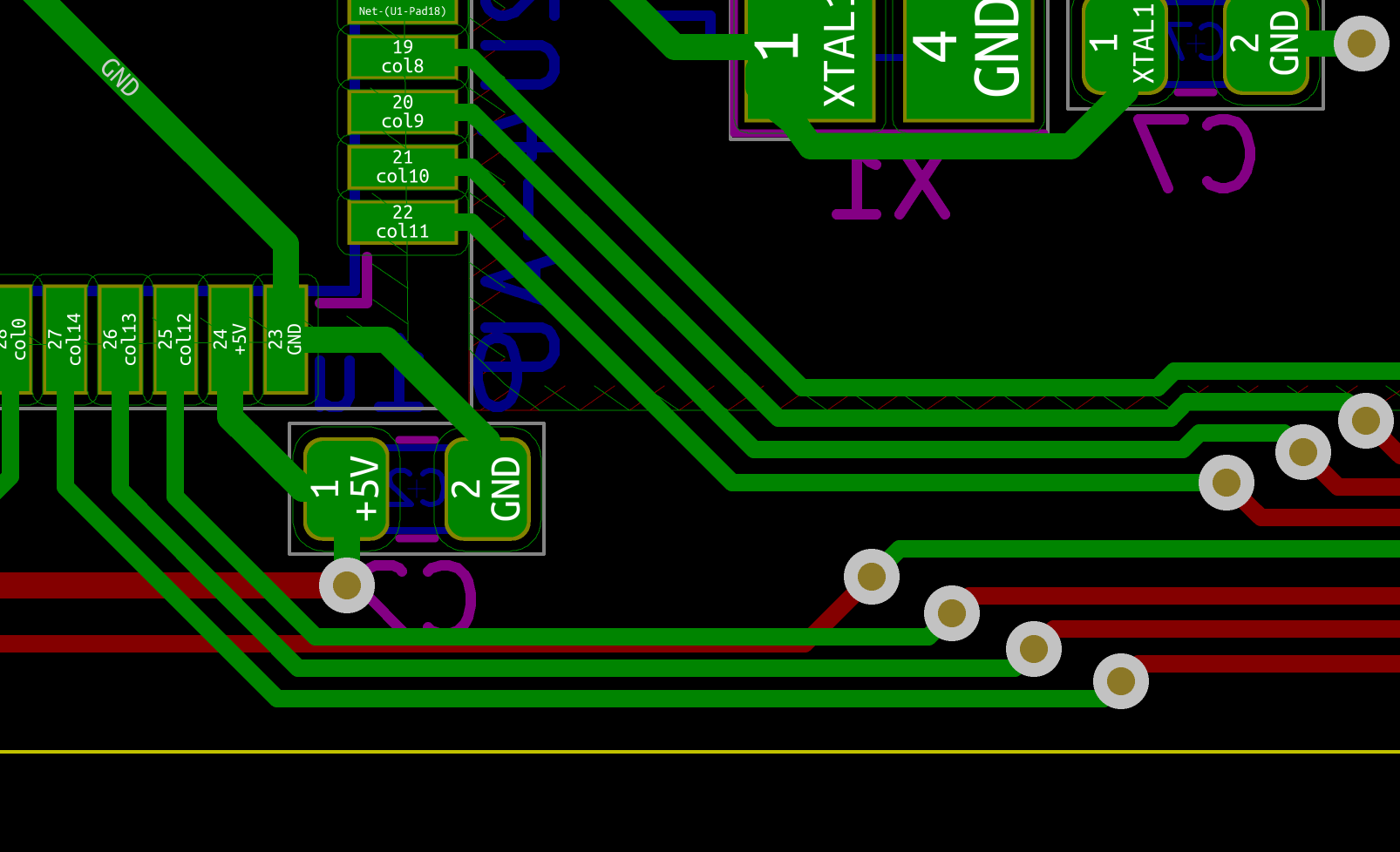
While doing that, make sure to not route the tracks too close to the border (or check the manufacturer clearance first). Then, keep tracing all tracks to their respective columns with the same kind of layout:
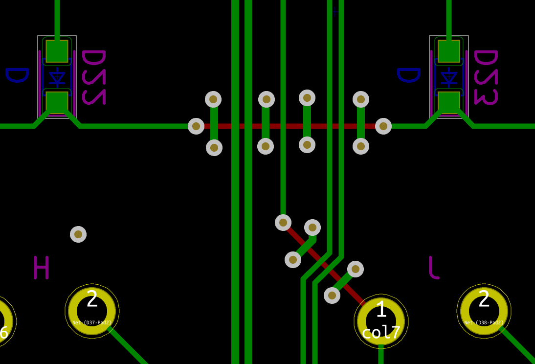
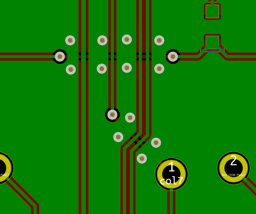
And finally, the last part of the matrix to be connected are the remaining rows (from row0 to row3, as row4 is already connected). There are multiple solutions (in fact any column in-between would work). But once again, I’m afraid I’ll have to rearrange the MCU pads:
There’s row3 at a very short distance from pad 1, so it makes sense to connect it there. I’m going to connect the rows from the left part and down between row3 and row4 as this will minimize the number of crossings:
But then arriving to the MCU it’s clearly not in the right order:
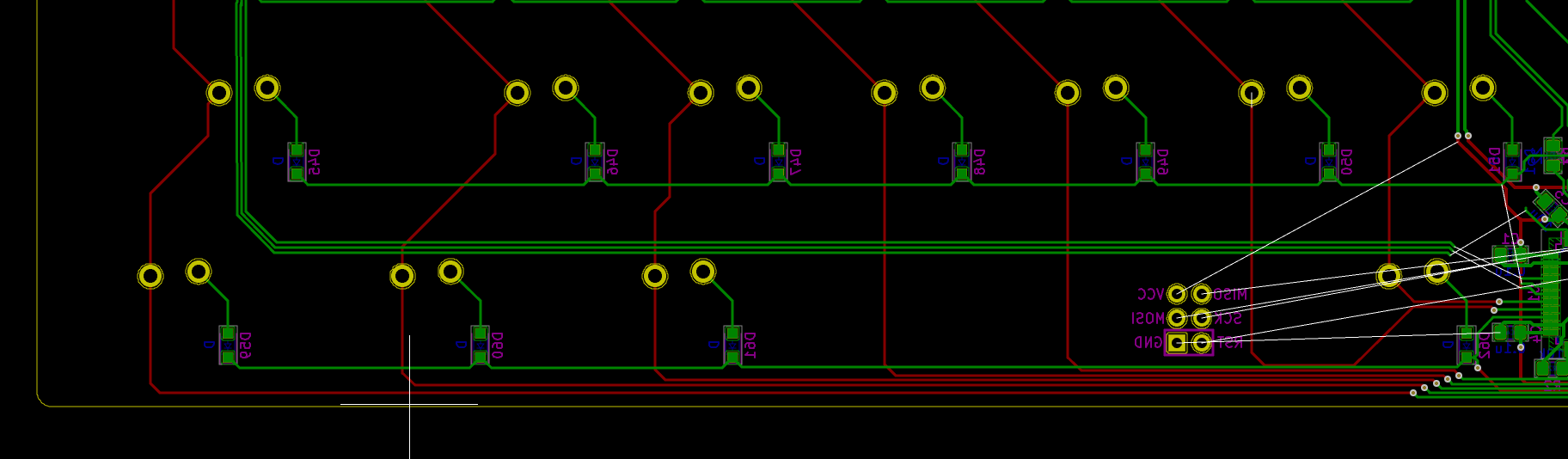
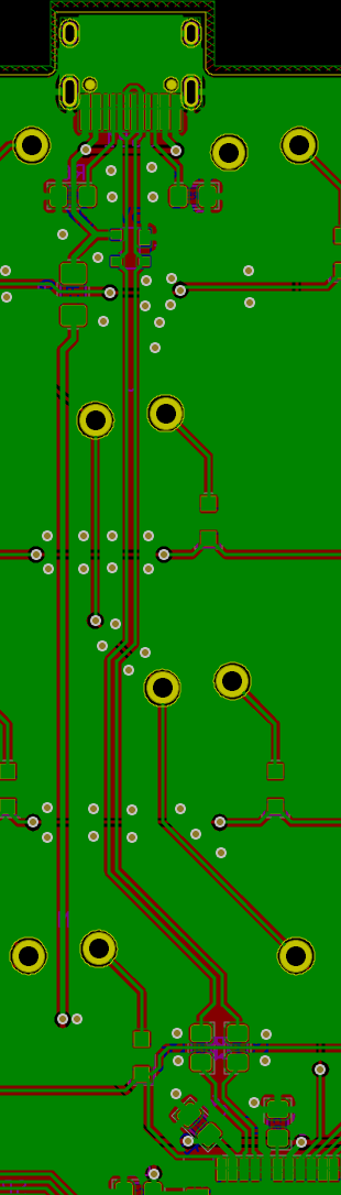
Let’s rearrange the rows in top down order in the schematic:
And after updating the PCB from the schematic, I can finally connect the remaining rows:
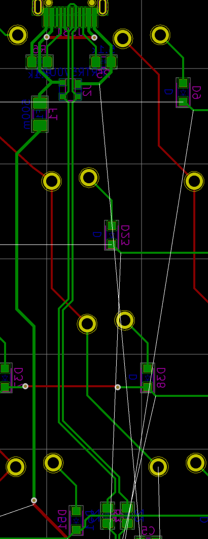
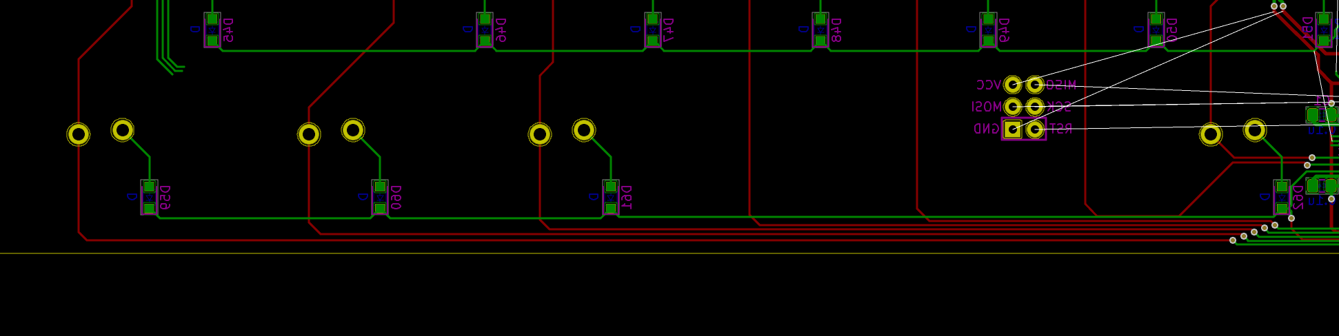
Last remaining bits
I still need to connect the reset button and the ISP header. Once everything has been done, it’s just a matter of finding its natural location (close to their assigned pads) and orientation (to minimize tracks crossings):
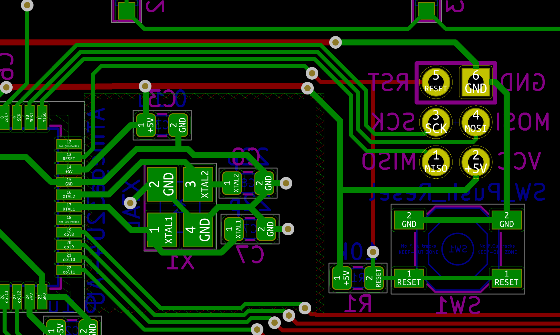
I had to divert col8 around the reset button and ISP header because it was too much in the way, but in the end it was possible to connect those components without too many vias.
Checking everything is right
Before going any further, I need to check the routing is correct. It’s easy to forget a connection or to cross two traces without noticing. Hopefully, Kicad has the Design Rules Checker feature which allows to check all those mistakes, but also the manufacturer clearances.
It can give the following errors:
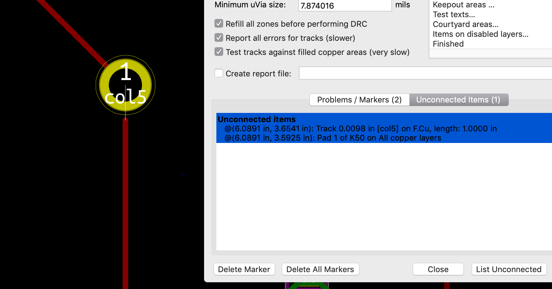
Thankfully this one is easy to fix.
Making the board a bit nicer
When looking at the 3D rendering of the PCB, you can notice the following issues:
- switch pads are not displayed on the front face (it’s just a matter of design preferences)
- the switch key name is not displayed anywhere (it’s nice to be able to know what key it is when soldering or troubleshooting)
- same for the ISP header
Let’s edit the footprints to remove the solder-mask on the top layer pads, but also display the switch value at least on the back.
Open the footprint editor, locate the Alps-1U footprint and select the left pad:
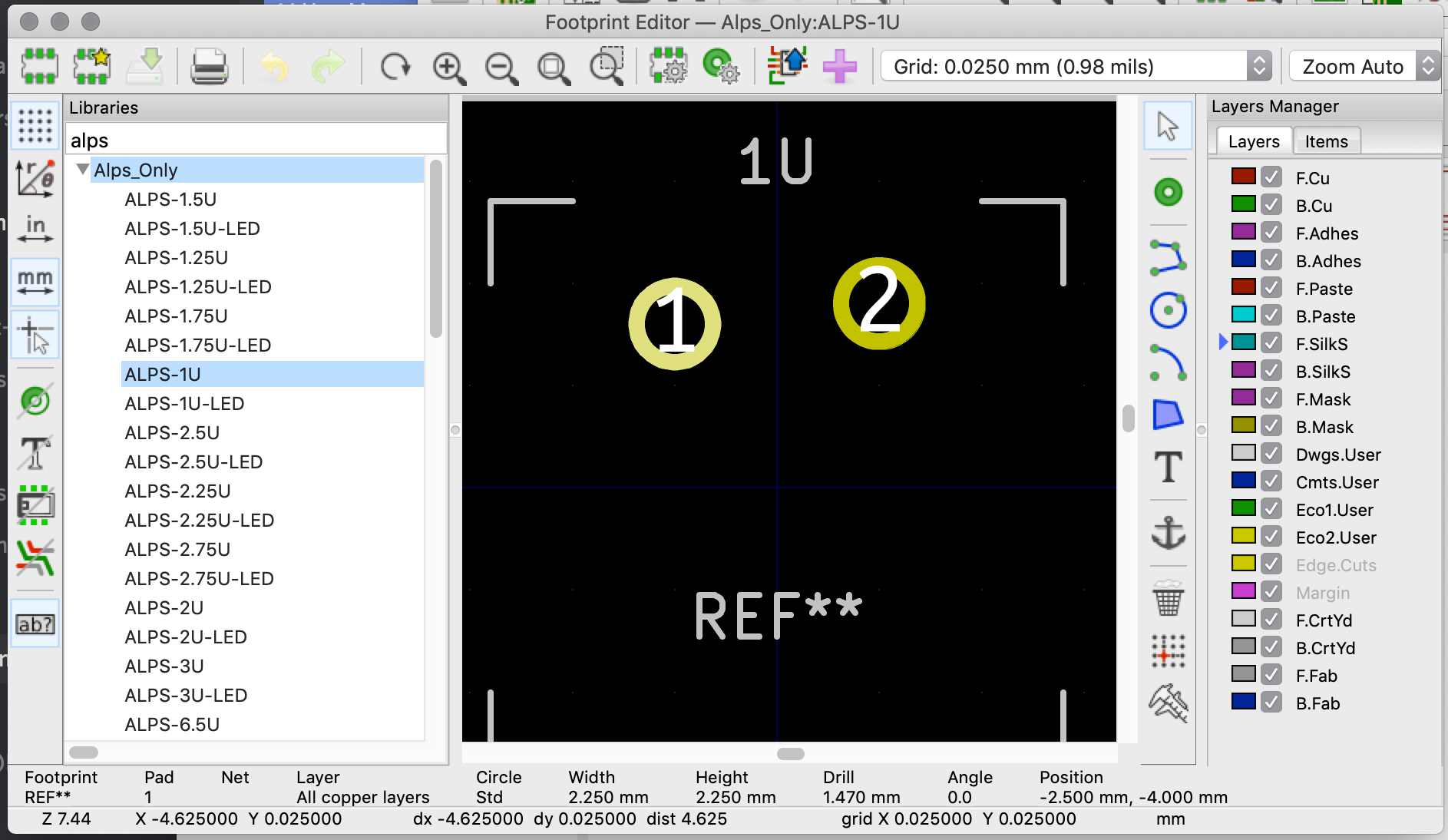
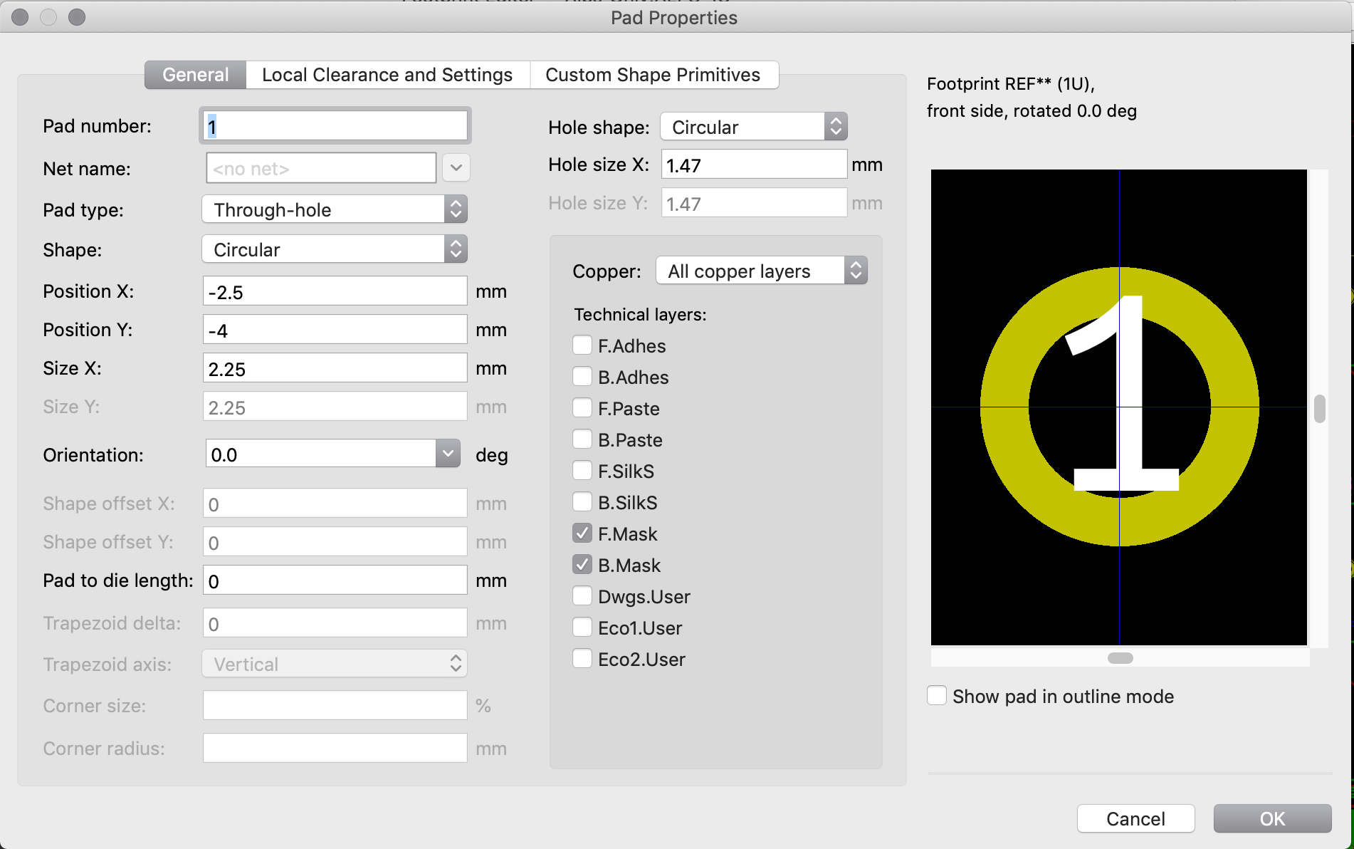
Edit the pad properties (e shortcut), and make sure that both F.Mask and B.Mask are checked:
Do the same for the second pad. Then place a new text near the top of the footprint enter %V in the Text entry box (that will reflect the component value, which happens for our switch to be the key name or symbol), chose the B.SilkS layer and check the mirrored checkbox:

If you also want the key name to be displayed on the front, add another text but chose the F.SilkS layer and unselect the mirrored checkbox.
Save the footprint, then do the same for the other footprint sizes.
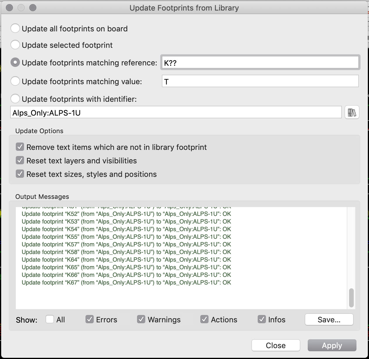
Once done, the PCB needs to be updated. In the PCB editor, select the Tools → Update Footprints from Library. In the dialog box, select all components with reference K??, check the three checkboxes so that all the text components will be updated and press update:
Check the 3D Viewer to see the rendered silkscreen on the front and back:
Unfortunately, we did this in the ai03 library so the modification can’t be committed to our PCB repository, because this library was added as a git submodule. Hopefully, I did the modifications in a fork of ai03 library (sorry, only Alps, no MX), so instead of adding ai03 submodule, you can add mine: git@github.com:masterzen/MX_Alps_Hybrid.git. And if you followed this article from the beginning, you can update the submodule with mine (see the How to change git submodule remote).
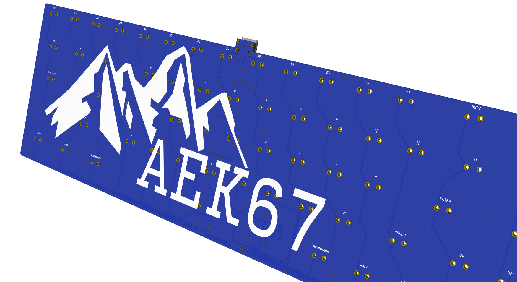
But wouldn’t it be a really cool PCB without at least a few silkscreen art?
The idea is to draw a vector logo (for instance in Adobe Illustrator or Inkscape), then import it as a footprint in Kicad.
Since this is an Alps based board, I thought it would be nice to have a mountain silhouette as the logo. Because I’m unable to create such art by myself, I downloaded a nice mountain wireframe in SVG from the Creative Commons Clipart website, loaded it in Inkscape and added the keyboard name (I had to rework the SVG to fix a few issues from there to there). Since this will go in the F.SilkS layer, I named the Inkscape layer F.SilkS:
![]()
If you want to add text, make sure to convert the text to paths (with the Object to path inkscape function), otherwise it won’t be imported.
Save the file into the format Inkscape SVG. Kicad doesn’t yet support importing SVG files directly, so we first have to convert the vector file to a format that Kicad can read. There are several possibilities:
- save a DXF from Inkscape and import it in Kicad. This works fine, but then any filled zone will be lost, and you need to recreate them in Kicad.
- use a converter tool like svg2mod or svg2shenzen.
I tried both method, and I won’t recommend the first one, because it is really painful to recreate all the zones in Kicad. Instead I’m going to show how to convert the SVG to a format Kicad can understand.
I wasn’t able to make the svg2shenzen Inkscape extension work correctly on my mac, so I resorted to using svg2mod which worked fine.
First install this tool with pip3 install git+https://github.com/svg2mod/svg2mod. Then run it on the svg file:
% svg2mod -i logo.svg -o ../local.pretty/logo -f 0.85 --name logo
Parsing SVG...
No handler for element {http://www.w3.org/2000/svg}defs
No handler for element {http://sodipodi.sourceforge.net/DTD/sodipodi-0.dtd}namedview
No handler for element {http://www.w3.org/2000/svg}metadata
transform: matrix [4.9686689, 0.0, 0.0, 5.4800484, -251.10361, -536.90405]
transform: matrix [0.05325035, 0.0, 0.0, 0.0482812, 50.5374, 97.974326]
transform: matrix [0.05325035, 0.0, 0.0, 0.0482812, 50.5374, 97.974326]
transform: matrix [0.05325035, 0.0, 0.0, 0.0482812, 50.5374, 97.974326]
transform: matrix [0.05325035, 0.0, 0.0, 0.0482812, 50.5374, 97.974326]
transform: matrix [4.9451996, 0.0, 0.0, 6.2660263, 266.42682, -668.87041]
Found SVG layer: F.SilkS
Writing module file: ../local.pretty/logo.kicad_mod
    Writing polygon with 5 points
    Writing polygon with 7 points
    Writing polygon with 22 points
    Writing polygon with 161 points
    Inlining 1 segments...
      Found insertion point: 0, 6
    Writing polygon with 22 points
    Writing polygon with 21 points
    Writing polygon with 28 points
    Inlining 1 segments...
      Found insertion point: 0, 0
    Writing polygon with 84 points
    Writing polygon with 31 points
This produces a Kicad footprint, which we can view in the footprint editor:
![]()
Note that I created it in the local library I used earlier to be able to commit it in my repository.
Next, place this footprint (o shortcut) on the PCB:
![]()
Unfortunately it isn’t possible to resize a footprint. The only way to resize such footprint is to regenerate it with a different resizing factor in svg2mod (the -f argument in the command above). This requires a few trials before finding the correct factor.
Let’s also do a small back-side logo. With the exact same logo, it is possible to flip it in Inkscape, rename the layer to B.SilkS, and finally save the SVG to another file. When converting the small logo to a Kicad footprint, make sure to use a very small -f factor (0.15 exactly). I can then place it on the PCB:
![]()
Finally, I’ve also added a small copyright and version number text on the B.SilkS layer.
The result
Here’s the result so far:
![]()
And the back:
![]()
To ground fill or not
I’ve seen a lot of 2-layers keyboard PCB design that use ground fills on both faces (not that the ai03 tutorial is not doing this). I believe the attempt here is to implement some kind of EMI reduction or crosstalk reduction. I tend to think it might be counterproductive to have such ground fills (or pour). First those won’t reduce EMI, only proper bypass/decoupling capacitors, conscious routing of high frequency trace (to minimize loops area), or using a ground grid scheme can help reduce EMI on 2 layers board (and on 4+ layers boards, using uninterrupted ground/power planes). Some will say that it helps for heat dissipation, or that they are forced to use ground fills for manufacturing reasons or that they paid for the copper, so better use all of it. Those might be valid reasons, but for such project a ground fill might really be overkill.
Don’t get me wrong, on a multilayer PCB, having uninterrupted ground planes is essential to reduce EMI. But on 2-layers PCB, it will be hard to have an uninterrupted ground (hence we talk about ground fill, not plane). Any slot in the ground fill that would interrupt a return current will just become an antenna. A ground fill might reduce cross-talks between traces, but it might also act as an antenna if it’s too thin and long. So if you want to add a ground fill, just make sure you take this into account.
That’s the reason we routed GND as a trace earlier, at least there’s an uninterrupted return path for the current. We could stop the design here and produce the board as is, it would definitely work.
Still for the exercise, I’m going to try to add a ground fill on both faces, but doing so correctly (or at least trying).
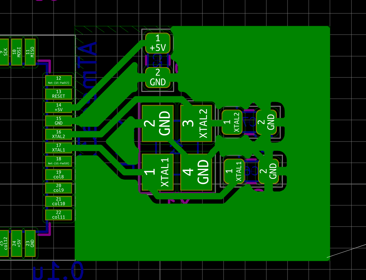
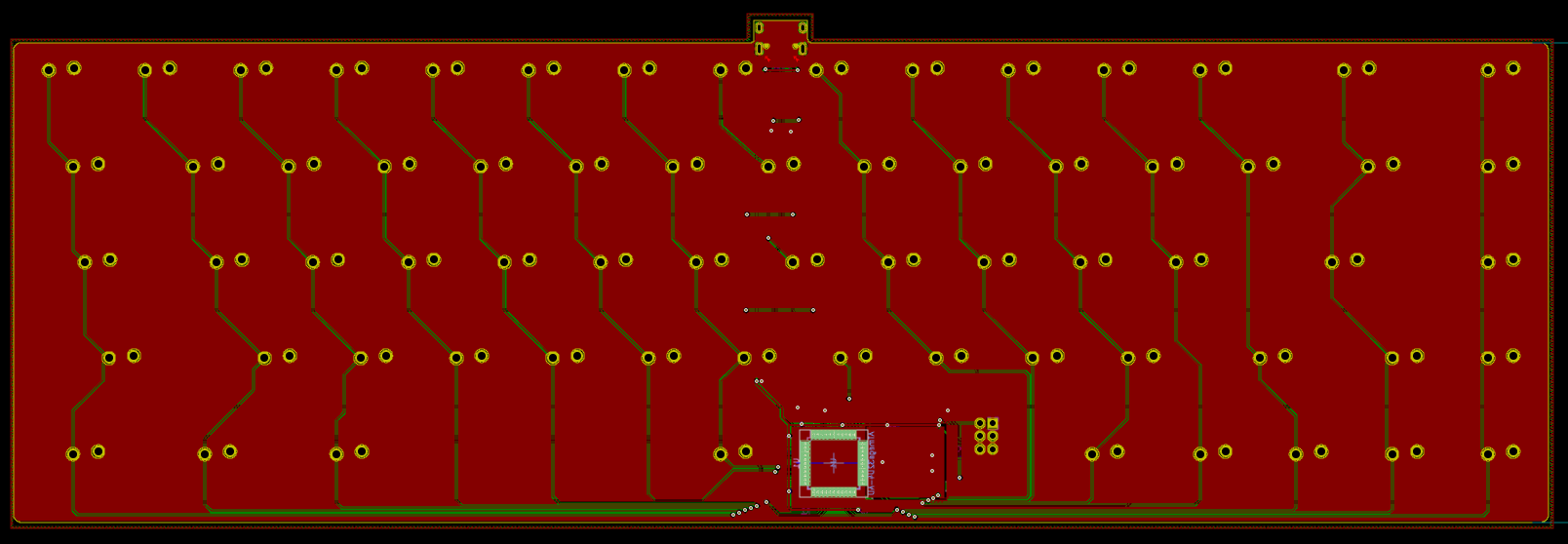
Let’s see how we can add a ground pour. In kicad use the Add Filled Zone tool and draw a large rectangle in the B.Cu layer around the whole PCB. To ease drawing, it’s better to use a 20 mils grid settings:
Keep going around the board:
And connect back to the starting point. This gives this:
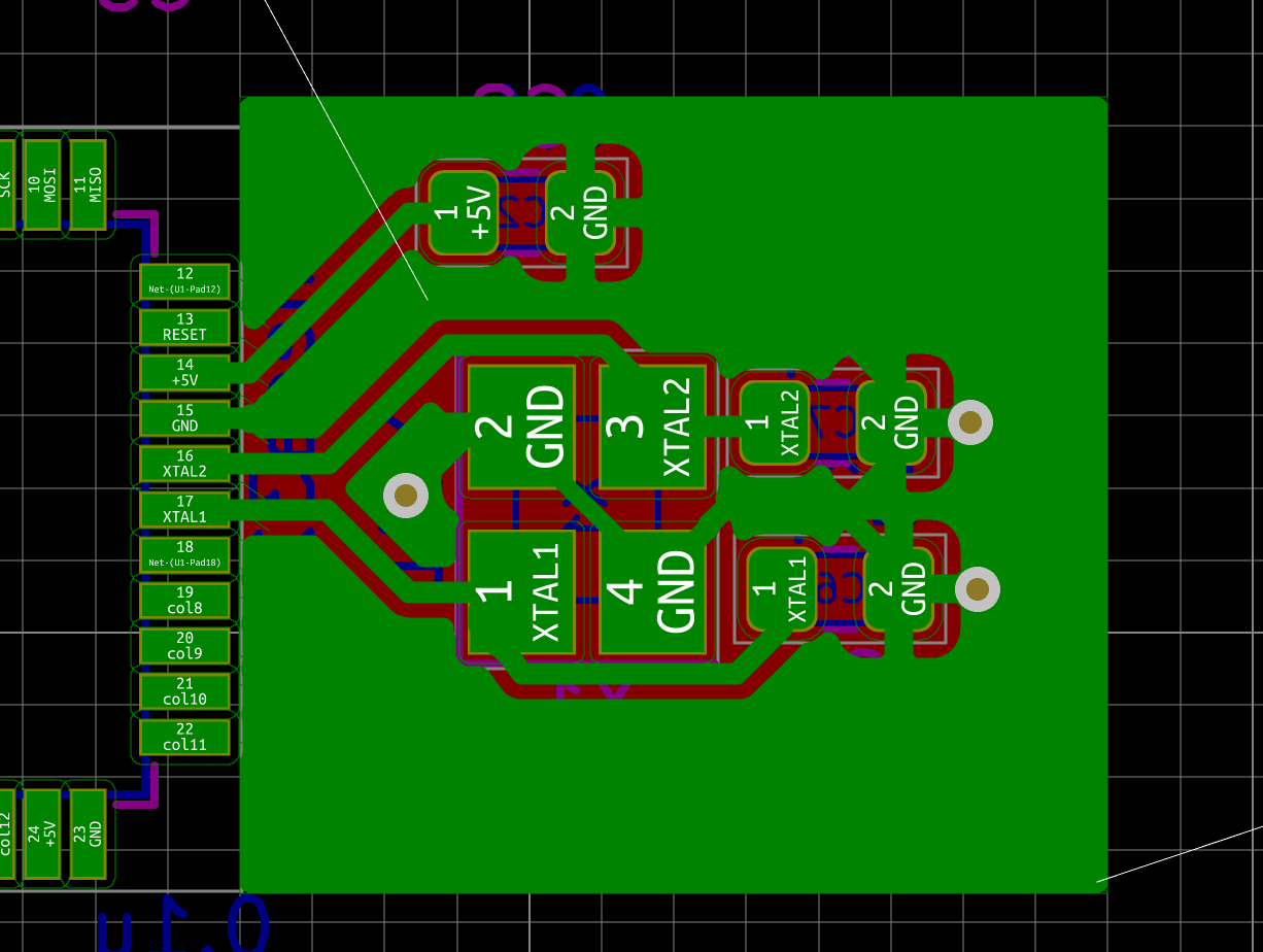
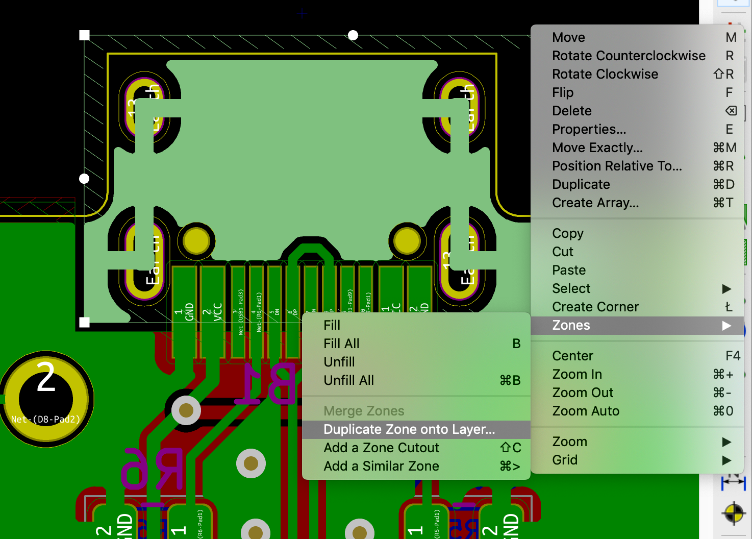
This is far from being perfect, because it merged the crystal oscillator ground island we designed earlier. I have to add a keep out zone to disconnect the island. This can be done by right-clicking on the ground zone and choose Zones → Add a Zone Cutout, then draw a rectangle around the crystal oscillator ground zone, spaced by 20 mil:
Next, let’s duplicate the same copper fill on the other side by going again in the zone contextual menu and choosing Duplicate Zone onto layer and chose GND on F.Cu:
Note that when creating a zone, make sure to select the Pad connection thermal relief option. A set of clearance parameters that works fine is 6 mils for the regular clearance, 10 mils of minimum width and 20 mils for both thermal clearances. The thermal clearance and pad connection are very important settings, without those, hand-soldering the PCB might be difficult as the ground fill copper would dissipate the soldering iron heat and the solder wouldn’t flow correctly. If the PCB is to be assembled at a factory then it wouldn’t be an issue.
Let’s look what we can do to make the copper fill better. First we have to make sure the copper fills are properly grounded together (they need to have the same potential to not be a gigantic antenna) by stitching vias from there to there. This will reduce the plane capacitance, but that’s not an issue since we have plenty of decoupling capacitors around the MCU. The idea is to reduce the potentiality of any part becoming an antenna. Place a few vias from there to there or use the Via Stitching kicad plugin to do that. Here’s an example with the Via Stitching plugin with a grid of 32 mm (it’s possible to add more vias, but there’s no need to make a Swiss cheese):
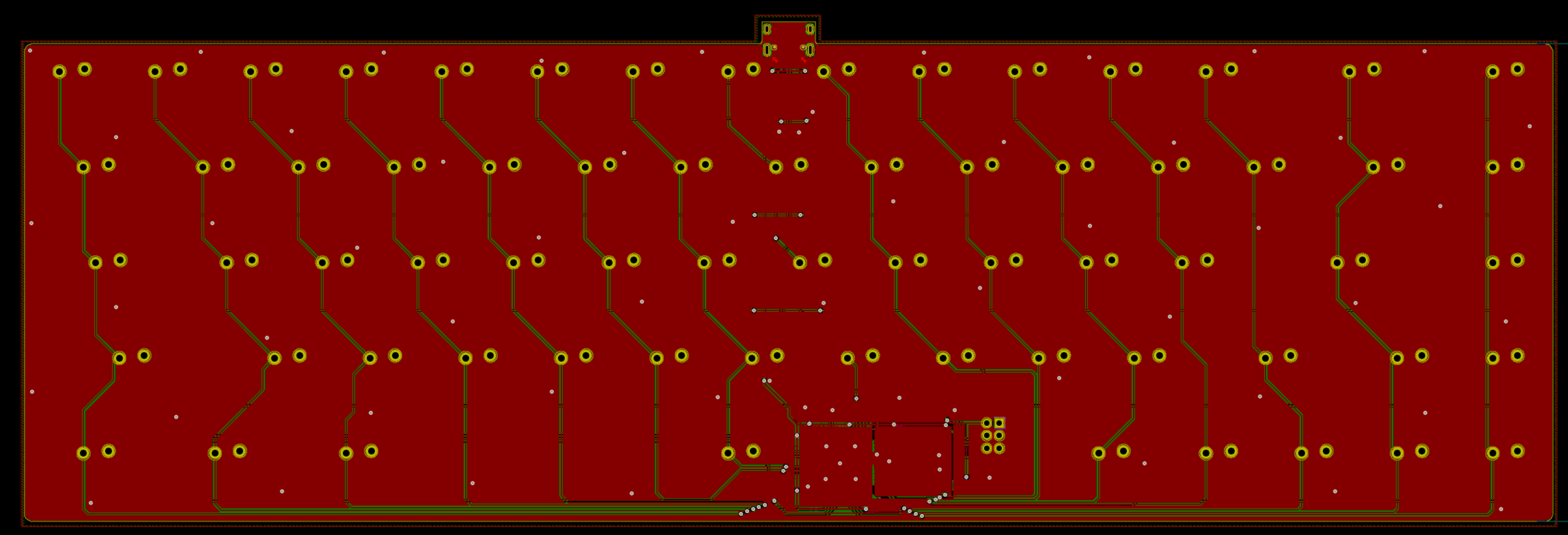
It’s not finished yet. If the return current of the D+/D- goes into the F.Cu ground fill back to the USB connector, the path of least impedance (that’s the path of high frequency signals) would cross several horizontal traces. This isn’t good, the current loop area will be large (those return currents will have to turn around the obstacles increasing the loop area). The largest the current loop, the largest the electromagnetic emissions. To circumvent this issue, we can add a few pairs of vias around those horizontal traces that split the F.Cu plane. To do that, work in Do not Show Filled Zone mode and create small GND tracks and vias across the horizontal lines:
Going back to the visible Filled Zone mode, this would look like this:
Next, repeat that around all the zone splits that the differential pair crosses:
 ](/images/uploads/2020/05/pcb-route-all-vias-bridges.png)
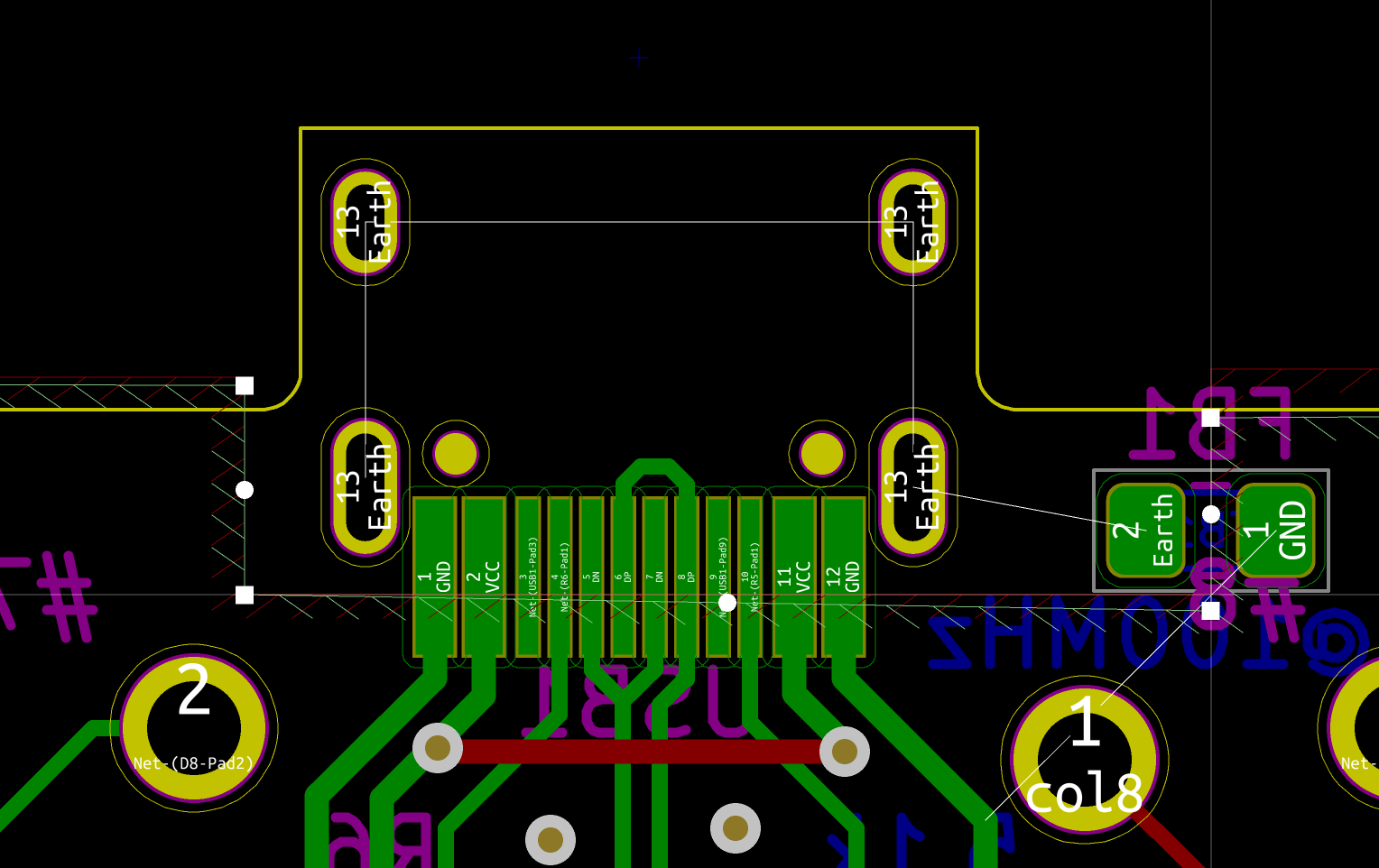
Revisiting the USB shield
In this series first part, I opted for an USB schema where I connected the shield and ground.
There are endless debates on the Internet about whether it’s correct or not to connect shield and ground. I did a lot of research, because I had the feeling that it might be wrong.
The USB cable shield is there to prevent electromagnetic outside noise from coupling with the USB data wires, but also to protect the outside world from noise that could be generated by the USB data wires. Additionally, the USB port shield can be susceptible to electrostatic discharge through the USB connector.
What makes the matter complex is that the USB norm doesn’t tell exactly what should be done. In fact, it depends on a number of factors, among them: is it the host or device? Is it bus powered? self powered? powered by mains? etc.
If we focus on this project, I’m building a keyboard PCB (so from an USB standpoint a device powered through the bus), which I plan to enclose in an aluminium case.
This PCB will be connected to a computer (what’s the point if not?), and thus the device signal ground will be the same as the host signal ground and the cable shield will be connected to the host shield. On desktop computers the host shield is usually connected to earth ground. On laptops, it really depends. Anyway, let’s assume that the host shield is somehow correct.
Connecting the USB signal ground GND to the USB port shield will have the drawback of possibly having a return current using the cable shield, negating the effect of the shield (the shield would possibly induce noise in the USB data lines). It would also mean that potentially the keyboard case would be also connected to the USB singal ground, which wouldn’t be great in case of an electrostatic discharge: a tension could then be seen on ground (the PRTR5V0U2X ESD protection device we use can protect VCC but not GND).
Ideally the USB port shield should be connected to the metallic case (by using an EMI gasket, a direct connection or through metalized holes and screws in the PCB). That’s one of the reasons more and more custom keyboards are using the Unified USB Daughterboard. When the USB port shield is connected to the case, this one protects the PCB from EMI (and also helps reduce EMI coming from the PCB), but it also contains any ESD and direct them to the host.
So, would the shield be fully disconnected from the USB GND? In fact, no that would be worst. In case of an ESD, an electrical arc could form between the case and any close traces of the PCB (well after the ESD protection device) risking damaging the components (because the surge wouldn’t go through anything that would prevent it).
After researching literature for a while (especially Henry W. Ott’s EMC book), I concluded that a good plan would be to redesign the electric schema of the USB shield, and this part of the PCB. The aim is to create a dedicated I/O ground plane under the USB port shield that would be connected to the PCB GND through a ferrite bead. The other option could be to use a RC filter built of a 1MOhm resistor and a 4.7nF capacitor. But there’s not a lot of room on the PCB at this place so the ferrite bead is a good option.
A ferrite bead is a small common choke component that exists in SMD form-factor. It acts as a kind of lowpass filter. This aim is to filter out the high frequency noise that could be coupled in the shield before it can reach the USB GND or couples to the data lines. Unlike what is somewhat thought it can also help reduce the effect of an ESD. ESD spectral density is roughly around 100-500 MHz. This frequency range is specifically filtered by ferrite beads (if you wonder why, it’s because the ESD high rise time generates high frequency harmonics).
I just added a new component a Ferrite_Bead_Small with an Inductor_SMD:L_0805_2012Metric_Pad1.15x1.40mm_HandSolder footprint:
Then after annotating the schema (without annotating everything again to not change all the references), and updating the PCB, the split I/O ground fill has to be created. This can be done by first resizing the GND ground plane like this:
Then I can place the ferrite bead footprint across the seam between the I/O ground plane and the GND plane. Next, I can create the new I/O plane:
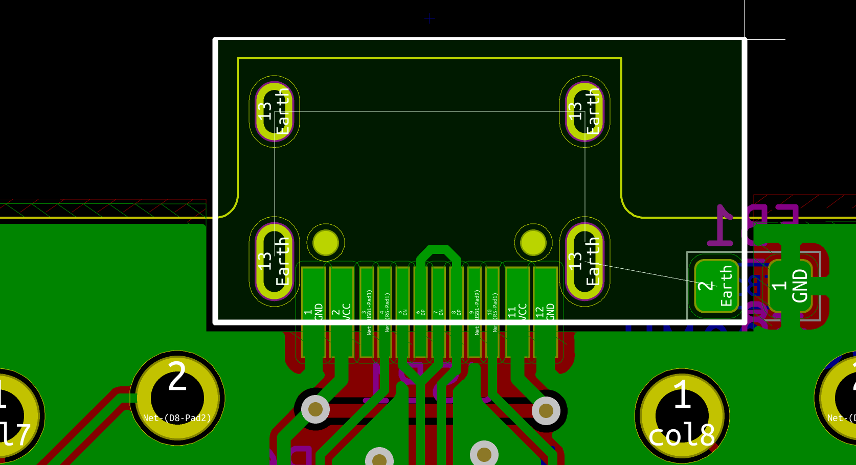
To ease creating the seam, use a coarse grid (for instance 10 mils). Finally, duplicate the zone on the F.Cu layer:
And finally, we need to make sure both planes are connected together (they are through the USB receptacle shield) by adding a few vias:
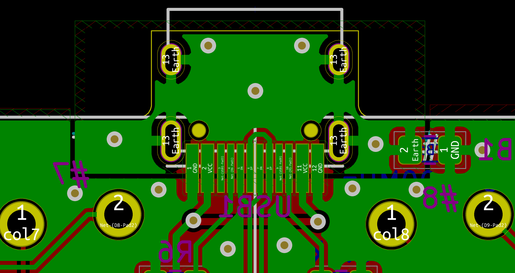
I also made the I/O zone symmetrical, to make it nicer.
How does it look finally?
Here’s the final PCB render:
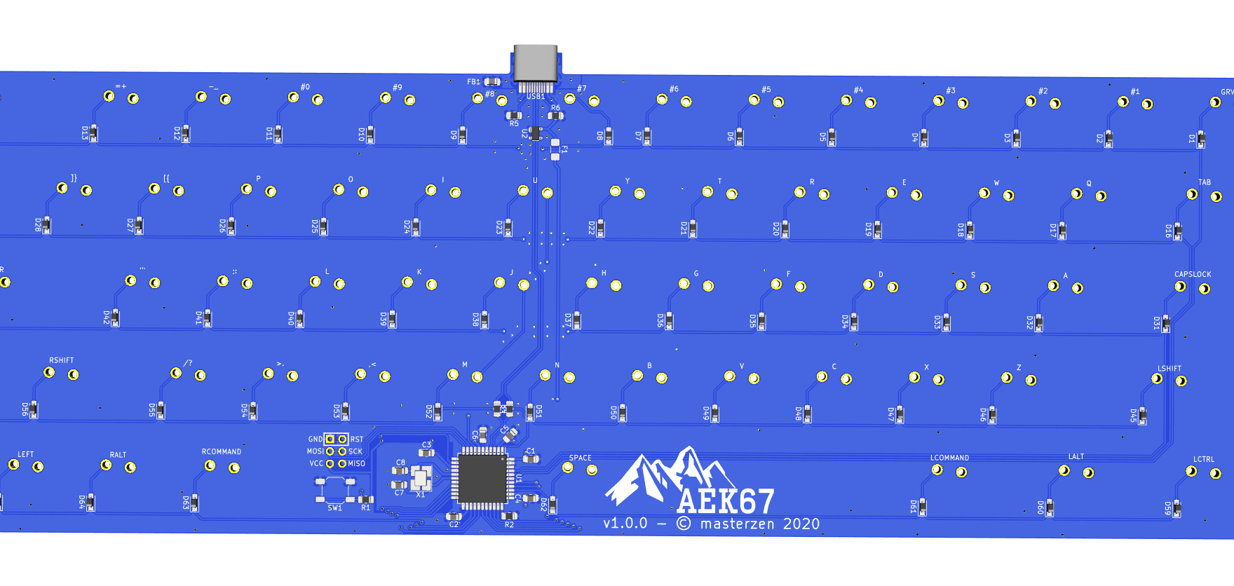
I quite like the result!
What’s cooking next
That’s all for today (it took so long to write this). In the next episode I’ll try to cover:
- producing manufacturing files and sending them to the manufacturer
- selecting the right components
- SMT soldering thechniques with a regular soldering iron
- creating the firmware
- testing the PCB
Thanks for following!
Comments