Designing a keyboard from scratch - Part 4
Welcome to the 4th episode of this series of articles about designing a full keyboard from scratch. So far we’ve seen:
- how to create the electronic schema of the keyboard controller in the first episode
- how to design the matrix and layout components in the second episode
- how to route the PCB efficiently in the third episode
I’ll now cover:
- production of manufacturing outputs
- ordering the PCBs
- selecting the correct components
- assembling the PCB
- creating the firmware
- and finally testing the PCB
This is again a long episode that took quite long time to write, sorry for the wait. Feel free to leave a comment if you have any questions or find anything suspect :)
Getting manufacturing files
We need to export our PCB out of Kicad and send it to the factory. Hopefully, all the factories out there use a common file format that is called the Gerber format.
This file format is a vectorial format that describe precisely the layer traces and zones, silk screens, and sometimes where to drill holes (some manufacturer require Excellon format). This has become a kind of interchange standard for PCB factories. This is an old file format that was used to send numerical commands to Gerber plotters in the 70s. Since then the format has evolved and we’re dealing now with Extended Gerber files.
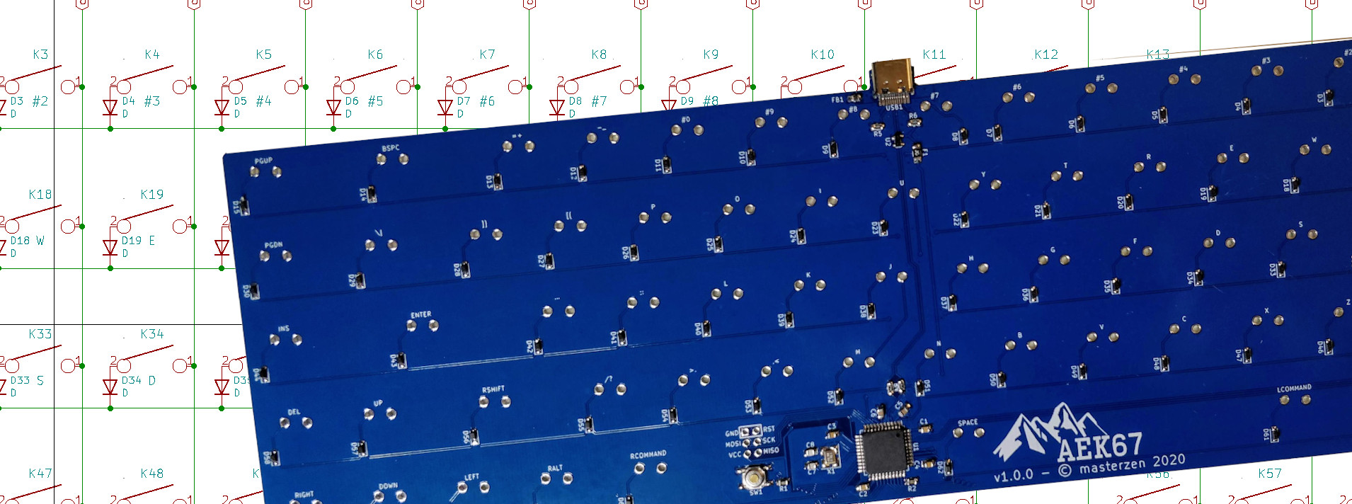
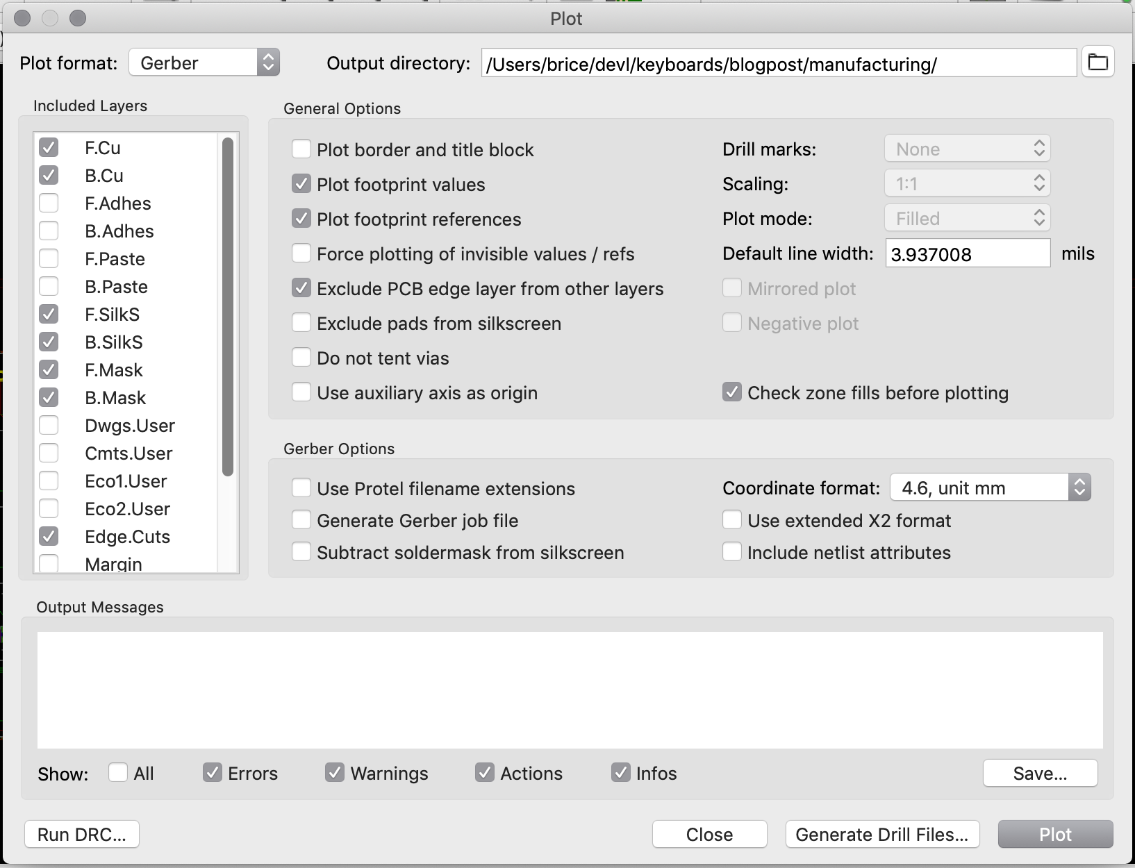
Back to my PCB, I can generate my set of Gerber files to be sent to the factory from pcbnew by going to File → Plot…. A new window opens where I can configure the output.
The options to set will depend on the manufacturer. Here’s a few manufacturer Kicad recommandations and settings:
- JLCPCB (China)
- PCBWay (China)
- Elecrow (China)
- OSHPark (USA)
- Eurocircuits (EU) - note that Eurocircuit reads directly the Kicad file, no need to generate Gerber files.
- Aisler (EU)
- Multi Circuit Board (EU)
- … There are many others, see PCBShopper for a comparator
Caution: different manufacturer have different tolerances and capabilities (for instance minimum track size, via size, board size, etc). Make sure you check with them if your PCB can be manufactured.
This time, I’m going to be using JLCPCB. Here’s the recommended setup for JLCPCB with Kicad 5.1:
For this project the following layers needs to be checked:
F.CuB.CuF.SilkSB.SilkSF.MaskB.MaskEdge.Cuts
The first two are for drawing the tracks and pads, the two next ones are the components reference and value indications (and the art), the two mask layers contains the zone where the copper layers will be seen (ie pads and holes), and finally the Edge.Cuts layer contains the board outline.
Make sure the chosen format is Gerber, then choose a sensible output folder (I like to put those files in a manufacturing subfolder of my PCB repository).
And additionnally those options need to be checked:
- Check Zone fills before plotting - to make sure zones have been recomputed
- Plot footprint values - because our switch footprints have the key name as values in the silkscreen
- Plot footprint references - because all the components except the switches have a unique reference (that will help locate the component when soldering)
- Exclude PCB Edge from other layers
When clicking on the Plot button, the files are generated (in the folder previously entered).
The next step is to generate the drill files, which contain the location where to drill holes (for both types of holes: mounting holes or for through-hole components, and for plated and non-plated holes). This can be done by clicking on the Generate Drill Files button next to the Plot button in the previous window:
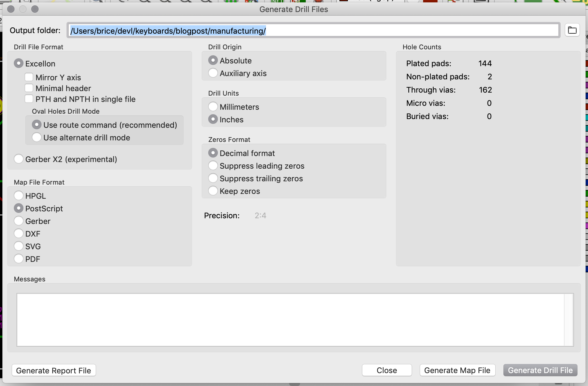
The important options to check are:
- Excellion
- Use route command
- Postscript
Generating the drill file is done by clicking on the Generate Drill File (oh that was unexpected :) )
This produces two new files in my manufacturing folder, one for the plated holes and the other ones for the non-plated holes. The manufacturing folder now contains:
aek67-B_Cu.gbraek67-B_Mask.gbraek67-B_SilkS.gbraek67-Edge_Cuts.gbraek67-F_Cu.gbraek67-F_Mask.gbraek67-F_SilkS.gbraek67-NPTH.drlaek67-PTH.drl
Now zip everything (cd manufacturing ; zip -r pcb.zip * if you like the command-line). That’s what we’re going to upload to the manufacturer.
Manufacturing
If you’re interested in PCB manufacturing, you can watch this video of the JLCPCB factory, you’ll learn a ton of things about how PCB are made these days.
So, the process is to upload the Gerber and drill files to the factory. But first it’s best to make sure those files are correct. Kicad integrates a Gerber viewer to do that. It’s also possible to check with an online Gerber viewer like for instance Gerblook or PCBxprt.
The Kicad viewer can be launched from the Kicad project window with Tools → View Gerber Files. The next step is to load the gerber files in the viewer with the File → Open ZIP file and point it to the pcb.zip file of the previous chapter.
This gives this result:
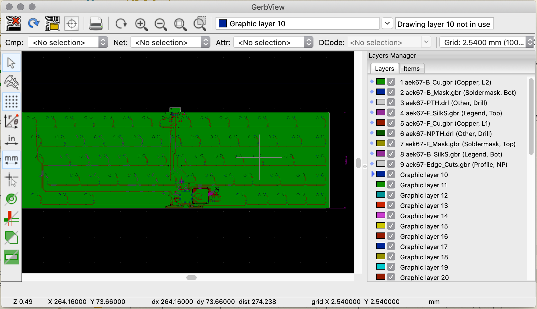
So, what to check in the viewer files?
- check that the files can be correctly opened
- check each layers independently
- for copper layers, check that the pads seems correct
- for soldermask layers, check that the soldermask doesn’t appear on pads
- for silkscreen layers, check that components’ references and values appear correctly, then check the silkscreen art and text if there are some.
Once this basic verification has been done, it’s time to upload the zip file to the manufacturer website. Once the file is uploaded, the site will display the gerber file. Make sure to check again the layers, as this time it’s the manufacturer interpretation of the files. With JLCPCB the interface looks like this:
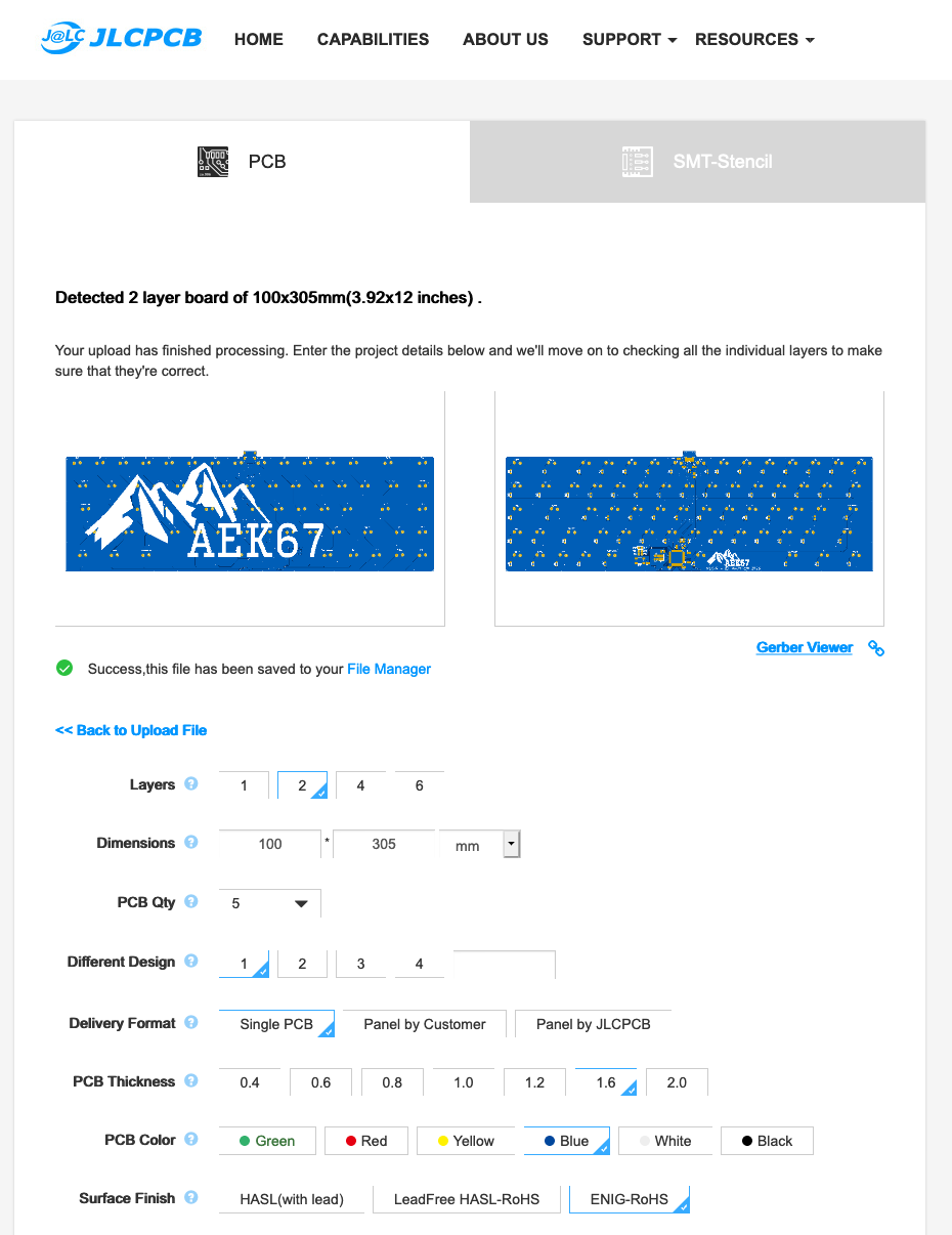
In this screenshot, I have omitted the price calculation and the bottom part (we’ll get to this one below). You can see the gerber view, and most manufacturer host an online gerber viewer to make sure the files are correctly loaded.
Immediately below, there’s the choice of number of layers and pcb dimensions. Those two numbers have been detected from the uploaded file. Make sure there’s the right number of layers (two in this case), and that the dimensions are correct. If not, check the gerber files or original Kicad files edge cutout.
The next set of options deals with the number of PCB and their panelisation:
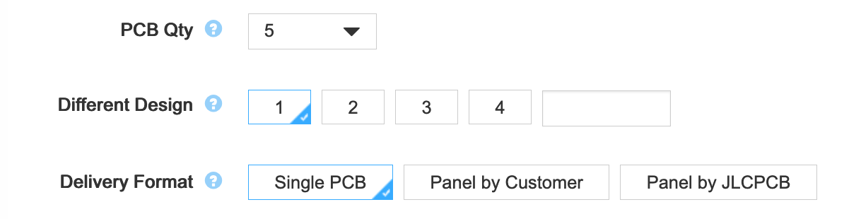
Paneling is the process of grouping multiple PCB on the same manufacturing board. The manufacturer will group several PCB (from either the same customer or different customers) on larger PCB. You can have the option of grouping your PCB the way you want, depending on the number of different designs you uploaded. On my case, this is straightforward as there’s only one design that doesn’t need to be panelized. Even though, I’m going to build only one keyboard, the minimum order quantity is 5 pieces. But that’s not as bad as it seems, because that will leave me the freedom of failing the assembly of a few boards :)
The next set of options are the technical characteristics of the board:
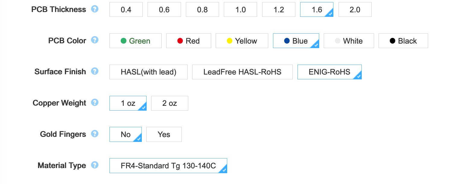
There we can change the thickness, color, finish, copper weight etc.
Those parameters are important so I need to explain what to choose. The PCB thickness represents the thickness of the FR4 fiber glass board sandwiched by the two copper layers which are later on etched to form the tracks. For a regular keyboard the standard is 1.6 mm. If you want to build a keyboard with more flex, you can opt for a 1.2 mm PCB. Note that in this case, it will not be possible to properly use PCB snap-in stabilizers (hopefully it won’t be an issue for screw-in stabilizers or plate stabilizers). Since this PCB is to be used in a regular keyboard, the default 1.6 mm is to be used.
The PCB color is a matter of preference of course. Just know that the final price is dependent on the chosen color. Most PCBs manufactured by JLCPCB are green, so this color is a lot cheaper (and take less lead/build time) than blue ones. Since the beginning of this series I was showing a blue soldermask so I decided to keep using a blue soldermask. I got a warning that it would mean two extra days of lead time.
Surface finish is how the pads and through-holes are plated. There are three possibilities, HASL, lead-free HASL, and ENIG. Technically the two first ones are equivalent.
The pads’ copper will oxidize with time at the contact with air. Those solderable parts of the PCB must be protected by a surface treatment to prevent oxidation. The HASL (Hot Air Solder Leveling) and its lead-free variant consist in dropping a small amount of solder tin-alloy on all the visible copper parts. ENIG or Electroless Nickel Immersion Gold is a plating process consisting in plating the copper with a nickel alloy and then adding a very thin layer of gold on top of it (both operations are chemical operations where the board is dipped in special solutions). I did test both options, and I really favor ENIG over HASL (despite the price increase). I found that it is easier to solder SMD components on ENIG boards than on HASL ones (the solder seems to better wet and flow, also the surface is completely flat on ENIG boards so it’s easier to place components).
The copper weight is in fact a measure of the copper thickness on each layer. The default is 1 oz, which means a thickness of 35 µm. Using a thicker copper layer would change the trace thickness and thus their electrical characteristics (inductance, impedance and such). The default of 1 oz is fine for most use cases.
Next gold fingers. This isn’t needed for most PCB (especially keyboards). Gold fingers are visible connection traces on the edge of the PCB that are used to slot-in a daughter card in a connector.
Finally for 2-layers boards, JLCPCB doesn’t offer to choose a different board material than regular FR4.
The next set of options are less important and some are straightforward:
I will just talk about castellation holes. Those are plated holes at the edge of the board. They will be cut in half in the process (if the option is selected). One of the use case is to join and solder two distinct pcb by the edge, using either solder joints or specialized connectors. This option is not needed for this project.
And finally the last option is the possibility to have the pcb separated by a piece of paper when packed. JLCPCB quality is reasonably good, but I had a few of my PCBs with partly scratched silkscreen or soldermask. It’s up to you to select or not this option (it increases the price because of the extra labor).
Before ordering, it is also possible to purchase assembly. In this case, all the components will be soldered at the factory (though they only support one face and only some specific parts, USB receptacles for instance are not available). If selected, you’ll need to provide the BOM and the parts position/orientation (Kicad can gnerate this placement file, but there are some recent Kicad versions generating files with bad parts orientations). Since this would spoil the fun of soldering SMD parts by hand, I won’t select it.
It’s also possible to order a stencil. A stencil is a metal sheet with apertures at the pads locations (imagine the soldermask but as a metal sheet), here’s an example:
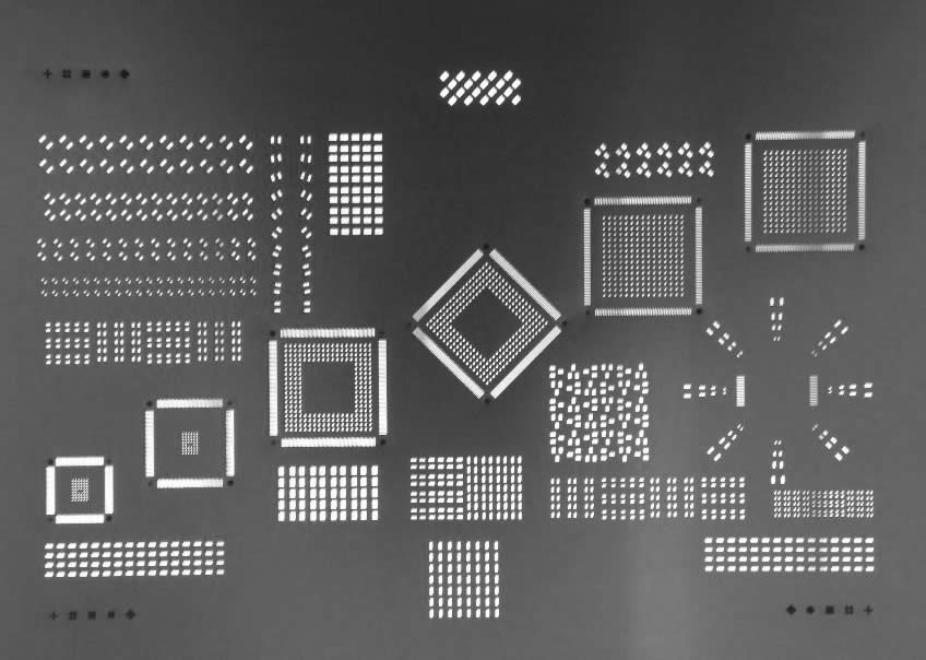
When soldering with a reflow oven or an hot air gun (or even an electric cooking hot plate)), the stencil is used to apply solder paste on the pads. This technique is demonstrated in this video. I don’t need this option either, as I intend to hand solder with a soldering iron the SMD components.
The next step is to finalize the order, pay and wait. Depending on the options (mostly the soldermask color), it can take from a couple of days to more than a week for the PCBs to be manufactured. Shipping to EU takes between one or two weeks depending on the chosen carrier (and the pandemic status).
A PCB without any components is of no use. So while waiting for the boards to be manufactured and shipped to me, let’s order the components.
Selecting parts
Kicad is able to generate a BOM list with the File → Fabrication Output → BOM File... This produces a CSV file. Note that it’s not a regular CSV where fields are separated by commas, instead they are using semicolon separators. This file can be loaded into a spreadsheet software. After cleaning it a bit (removing the switches and logos), it gives this kind of table:
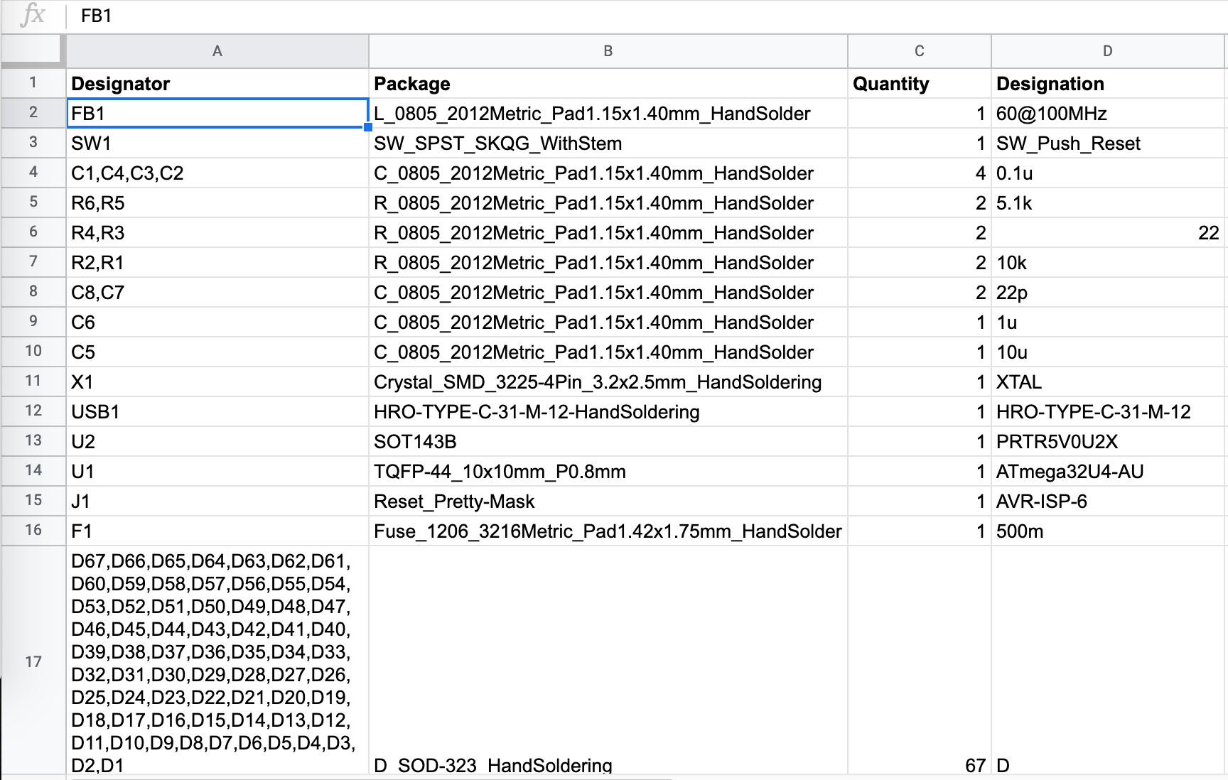
This will be of great help to know how many components I have to order to build one PCB (or the 5 ordered in the previous chapter).
So in a nutshell, for this keyboard, the following parts need to be sourced:
| Designation | Type | Footprint | Quantity |
|---|---|---|---|
| FB1 | Ferrite Bead | 0805 | 1 |
| SW1 | Reset switch | SKQG | 1 |
| C1-C4 | 100nF Capacitor | 0805 | 4 |
| C5 | 10uF Capacitor | 0805 | 1 |
| C6 | 1uF Capacitor | 0805 | 1 |
| C7, C8 | 22pF Capacitor | 0805 | 2 |
| R1, R2 | 10kΩ Resistor | 0805 | 2 |
| R3, R4 | 22Ω Resistor | 0805 | 2 |
| R5, R6 | 5.1kΩ Resistor | 0805 | 2 |
| X1 | 16 MHz Crystal | 3225 | 1 |
| USB1 | USB Connector | HRO-TYPE-C-31-M-12 | 1 |
| U2 | PRTR5V0U2X | SOT143B | 1 |
| U1 | Atmega 32U4-AU | TQFP-44 | 1 |
| F1 | PTC Fuse | 1206 | 1 |
| D1-D67 | Diode | SOD-123 | 67 |
First, let’s see where electronic parts can be bought. There are lots of possibilities. I don’t recommend sourcing from random stores on AliExpress, but instead ordering from professional vendors. You’ll be sure to get genuine parts (and not counterfeited components). Professional vendors will also store and ship correctly components in term of humidity and ESD protections.
I usually buy parts from the following vendors (because I’m based in the EU, I tend to favor European vendors):
- LCSC, this is the JLCPCB sister company. China located, they ship everywhere. Most of the time you can purchase in small quantities (ie > 10). They occasionally run out of AtMega32U4. There’s a risk of customs taxes when shipping to Europe.
- RS Components, ships from Europe (VAT included) with free shipping in France for week-end orders.
- TME, based in Poland (VAT included), very fast shipping to European Countries
- Mouser, they also ship from Europe for European customers.
- Digikey, ships from the US (subject to customs taxes for Europeans)
I usually order from LCSC, TME and RS. With a predilection for TME lately. Almost all those vendors carry the same kind of components, sometimes even from the same manufacturers (for the most known ones like Murata, Vishay, etc). On LCSC, you’ll also find components made by smaller Chinese companies that can’t be found anywhere else.
All those vendors also provide components’ datasheets which is very useful to select the right part. For all components, I’ve added a table with links to the parts on LCSC, TME and Digikey.
Diodes
The diodes are the simplest component to select. A keyboard needs basic signal switching diodes, the most iconic one is the 1N4148. I selected the SOD-123 package reference 1N4148W-TP from MCC.
| Reference | LCSC | TME | Digikey |
|---|---|---|---|
| D1-D67 | C77978 | 1N4148W-TP | 1N4148WTPMSCT-ND |
PTC Resettable Fuse
To select a PTC resettable fuse, one need to know its basic characteristics. USB is able to deliver at max 500 mA (because that’s what the 5.1 kΩ pull up resistors R5 and R6 says to the host), so ideally the fuse should trip for any current drawn above 500 mA. Based on this, I can select a part that has the 1206 SMD form factor and a reasonable voltage.
I selected the TECHFUSE nSMD025-24V on the LCSC site. It trips at 500mA, is resettable (ie once it triggers, it will stop conducting, but will become conducting again after the surge), and it can sustain up to 100A (which is large enough to absorb any electrical surge). This specific part is not available from the other vendors, but can be substituted by the Bell Fuse 0ZCJ0025AF2E (other manufacturer’s part can also match).
This component looks like this:
To summarize:
| Reference | LCSC | TME | Digikey |
|---|---|---|---|
| F1 | C70069 | 0ZCJ0025AF2E | 507-1799-1-ND |
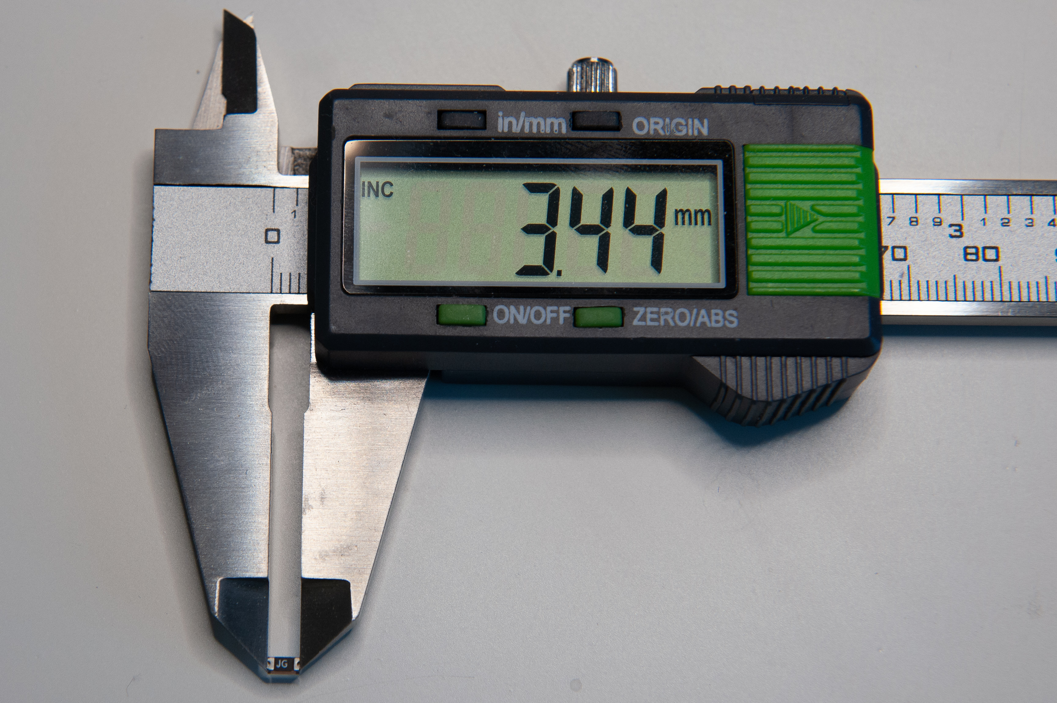
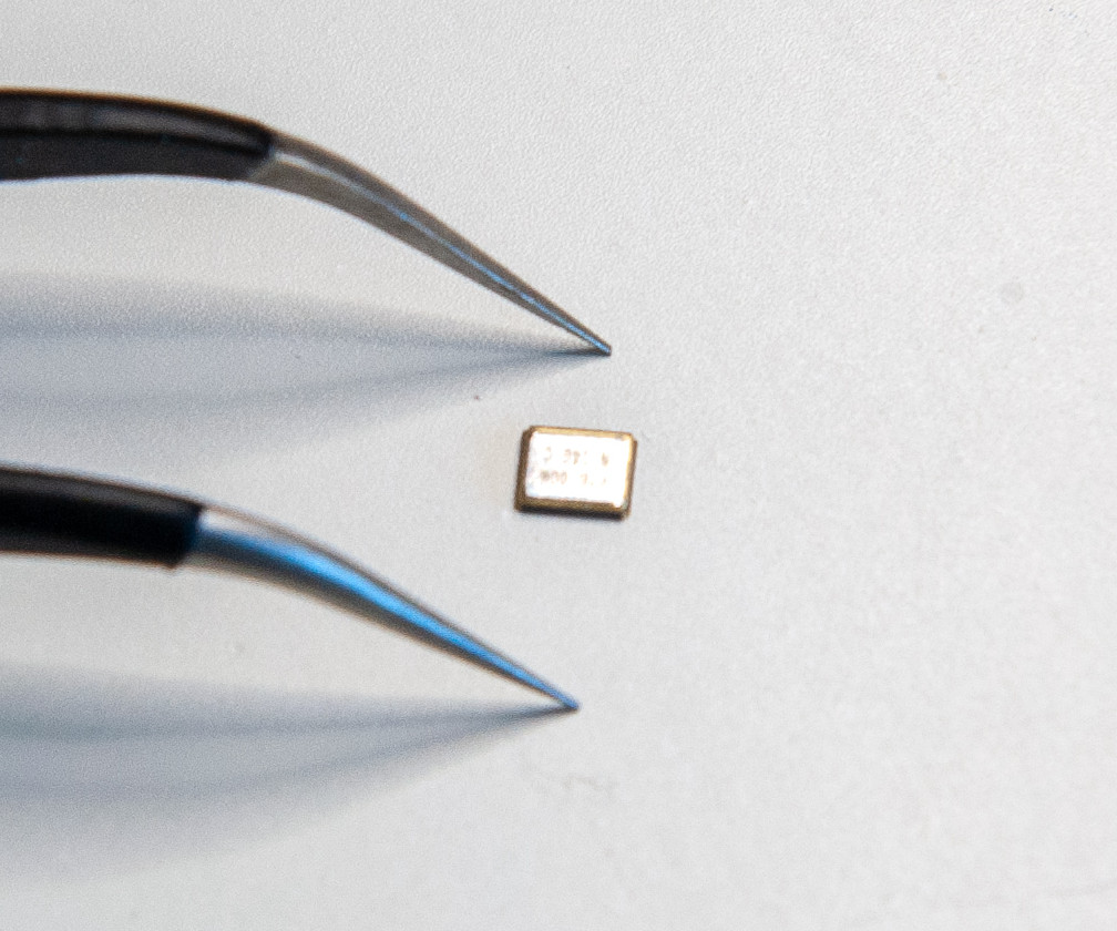
Crystal oscillator
The MCU I used by default is programmed to work with a crystal oscillator (or a ceramic resonator). To select such component, the main characteristics are it’s oscillation frequency (16 MHz here) and part size (3225). In LCSC, those parts are called Crystals Resonators, but in fact they are oscillators.
The next parameter is the frequency deviation in ppm. The lower is the better. Parts with the lowest ESR should also be favored.
In a previous design, I had selected the Partron CXC3X160000GHVRN00 but LCSC now lists this part as to not be used for new designs (I have no idea why, maybe this is an EOL product). So instead it can be replaced by either the Seiko Epson X1E000021061300, the IQD LFXTAL082071 or the Abracon LLC ABM8-16.000MHZ-B2-T, or the SR PASSIVEs 3225-16m-sr.
Here’s how a crystal oscillator looks like:
| Reference | LCSC | TME | Digikey |
|---|---|---|---|
| 16 Mhz Crystal | C255909 | 3225-16m-sr | 1923-LFXTAL082071ReelCT-ND |
Resistors
To choose resistors, the following characteristics matter:
- resistance (in Ω)
- tolerance (in percent)
- power
- package size
- temperature coefficient (short tempco) - or how much the resistance change with temperature. This parameter doesn’t really matter in our use case.
The tolerance is the amount of variation in resistance during manufacturing from one sample to another. The lower the tolerance is, the better the resistor has the indicated value, but the higher the price is.
For most of the applications, a 10% or 5% tolerance doesn’t matter, but for some applications you might want to go down to lower tolerance values like 1% or even 0.1%. I’ve selected 1% tolerance parts, but I believe it is possible to use 5% ones.
The power is the amount of power the resistor is capable to handle without blowing. For this keyboard, 125 mW (or 1/8 W) is more than enough.
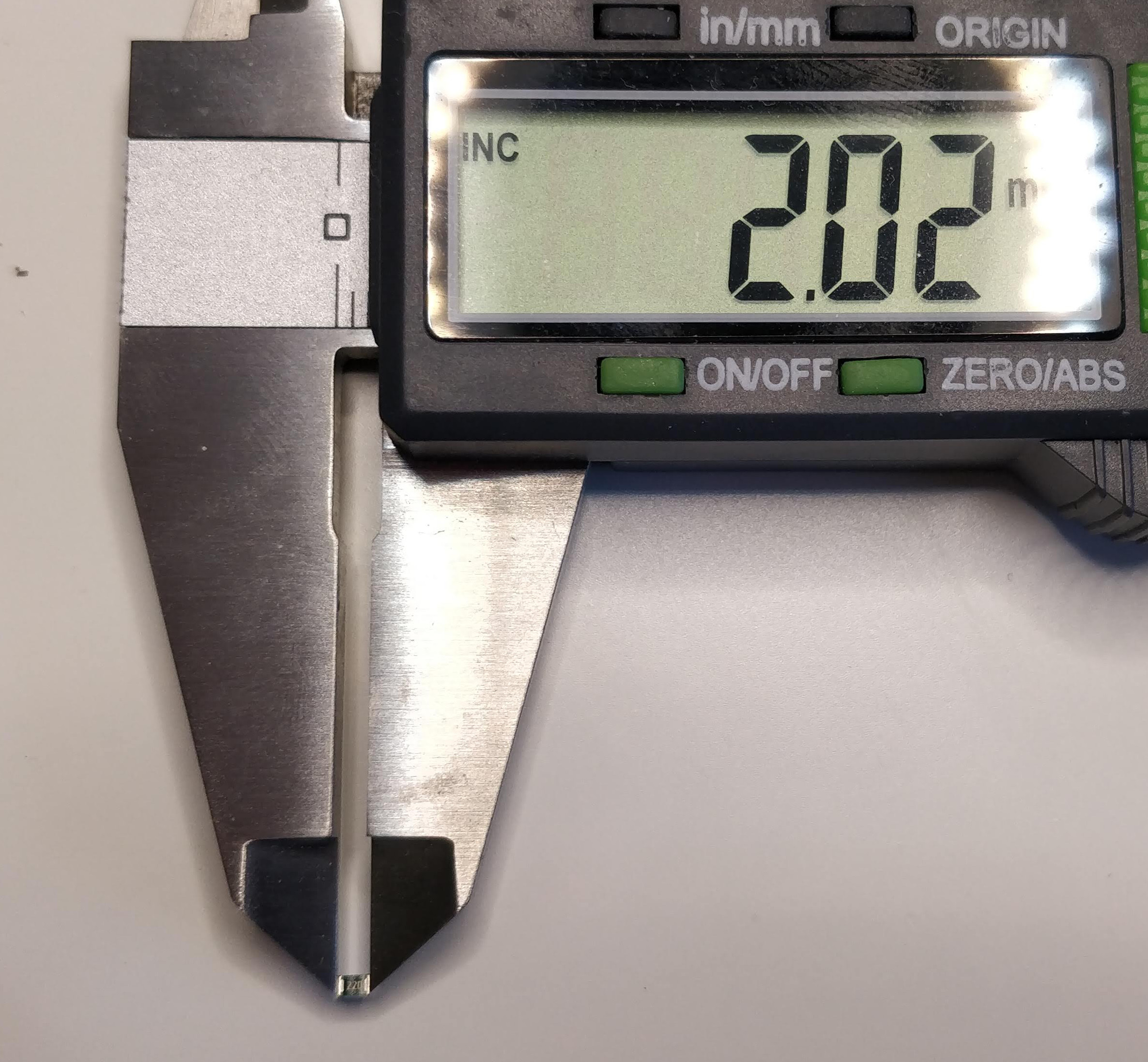
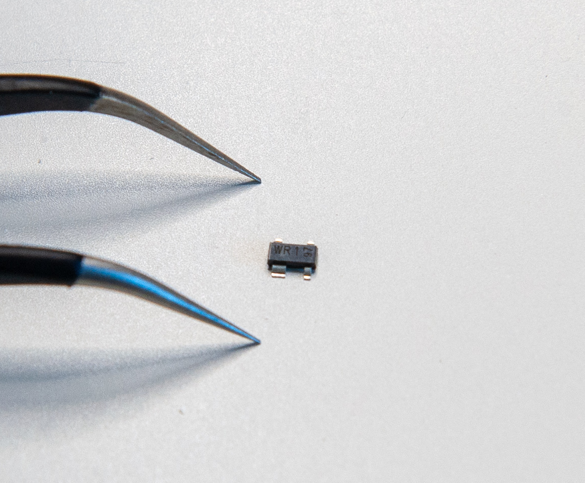
A SMD 0805 resistor (here it’s 22Ω) looks like that (yes that’s the small thing in the caliper):
Here’s a list of the selected part
| Reference | resistance | LCSC | TME | Digikey |
|---|---|---|---|---|
| R1, R2 | 10kΩ | C84376 | RC0805FR-0710KL | 311-10.0KCRCT-ND |
| R3, R4 | 22Ω | C150390 | CRCW080522R0FKEA | 541-22.0CCT-ND |
| R5, R6 | 5.1kΩ | C84375 | RC0805FR-075K1L | 311-5.10KCRCT-ND |
Note that some of those parts are available only in batch of more than 100 pieces. It is perfectly possible to substitute with parts that are sold in lower quantities as long as the characteristics are somewhat equivalent.
Capacitors
There are many type of capacitors of various conception and technology. For our decoupling/bypass SMD capacitors, MLCC (multi layered ceramic capacitors) are the best.
Here are the characteristics used to describe capacitors:
- capacitance (in F)
- tolerance (in percent)
- max voltage
- temperature coefficient
- package size
For decoupling and crystal load capacitors, it is not required to use a very precise capacitance, thus we can use the 10% tolerance. As far as this board is concerned, max voltage can be anywhere above 16V.
The temperature coefficient is (like for resistance) the variation in capacitance when temperature increases or decreases. For capacitors, it is represented as a three character code, like X7R, X5R, where:
- the first character is the lowest temperature the capacitor will work at (
Xis -55ºC for instance) - the second character is the max temperature (
5is 85ºC,7is 127ºC for instance) - the last character is the amount of capacitance change over the supported temperature range.
Rmeans +/- 15%, butVis about +-85% (ouch).
You might also find C0G (or NP0) capacitors. Those are completely different beasts (in fact it’s a complete different capacitor class), they are not affected by temperature at all.
It’s better to choose R over V variants (ie X7R is better than Y5V for instance). Since our keyboard temperature is not expected to increase considerably, X7R or even X5R can be selected. C0G parts are usually larger and harder to find in package smaller than 1206.
Among manufacturers, you can’t go wrong with AVX, Samsung, Vishay, Murata and a few others. I’ve selected Samsung parts in the table below.
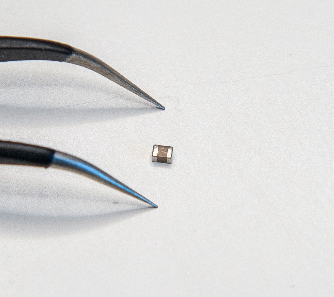
Here’s how a SMD 0805 capacitor looks like:
| Reference | capacitance | LCSC | TME | Digikey | Note |
|---|---|---|---|---|---|
| C1-C4 | 100 nF | C62912 | CL21B104KBCNNNC | 1276-1003-1-ND | |
| C5 | 10 uF | C95841 | CL21A106KOQNNNG | 1276-2872-1-ND | TME only have the X5R version |
| C6 | 1 uF | C116352 | CL21B105KAFNNNE | 1276-1066-1-ND | |
| C7, C8 | 22 pF | C1804 | CL21C220JBANNNC | 1276-1047-1-ND | lower capacitance are only available in C0G |
Ferrite bead
Choosing the right ferrite bead is a bit complex. One has to dig in the various reference datasheets. This PCB needs a ferrite bead that can filter high frequencies on a large spectrum (to prevent noise coupling in GND and ESD pulses). Ferrite beads characteristics are usually given as characteristic impedance at 100 MHz. That doesn’t give any clue about the characteristic impedance at over frequencies. For that, one need to look at the frequency diagrams in the datasheet.
What I know is that, the impedance at 100 MHz should be between 50Ω and 100Ω to be effective to filter out noise and ESD pulses. For the same reason, it also needs to resist to high incoming current.
After looking at hundreds of references, I finally opted for the Murata BLM21PG600SN1D .
Also, since I opted for a 0805 package, its current limit is in the lower part of the scale. I might probably change the PCB in an ucoming revision to use a 1206 sized ferrite bead to have it support higher currents.
| Reference | LCSC | TME | Digikey |
|---|---|---|---|
| FB1 | C18305 | BLM21PG600SN1D | 490-1053-1-ND |
The remaining parts
| Reference | LCSC | TME | Digikey | Note |
|---|---|---|---|---|
| PRTR5V0U2X | C12333 | PRTR5V0U2X.215 | 1727-3884-1-ND | |
| AtMega32U4-AU | C44854 | AtMega32U4-AU | ATMEGA32U4-AU-ND | |
| HRO-TYPE-C-31-M-12 | C165948 | not found | not found | |
| Reset Switch | C221929 | SKQGABE010 | CKN10361CT-ND | TME doesn’t carry the C&K switch, so substituted by the Alps version |
Here’s a picture of the PRTR5V0U2X, notice the GND pin that is larger than the other ones:
A bit more information on components
SMD components are packaged in tape reels. If you purchase less than a full reel (4000 to 5000 individual pieces), you’ll get a cut piece of the tape like this one:
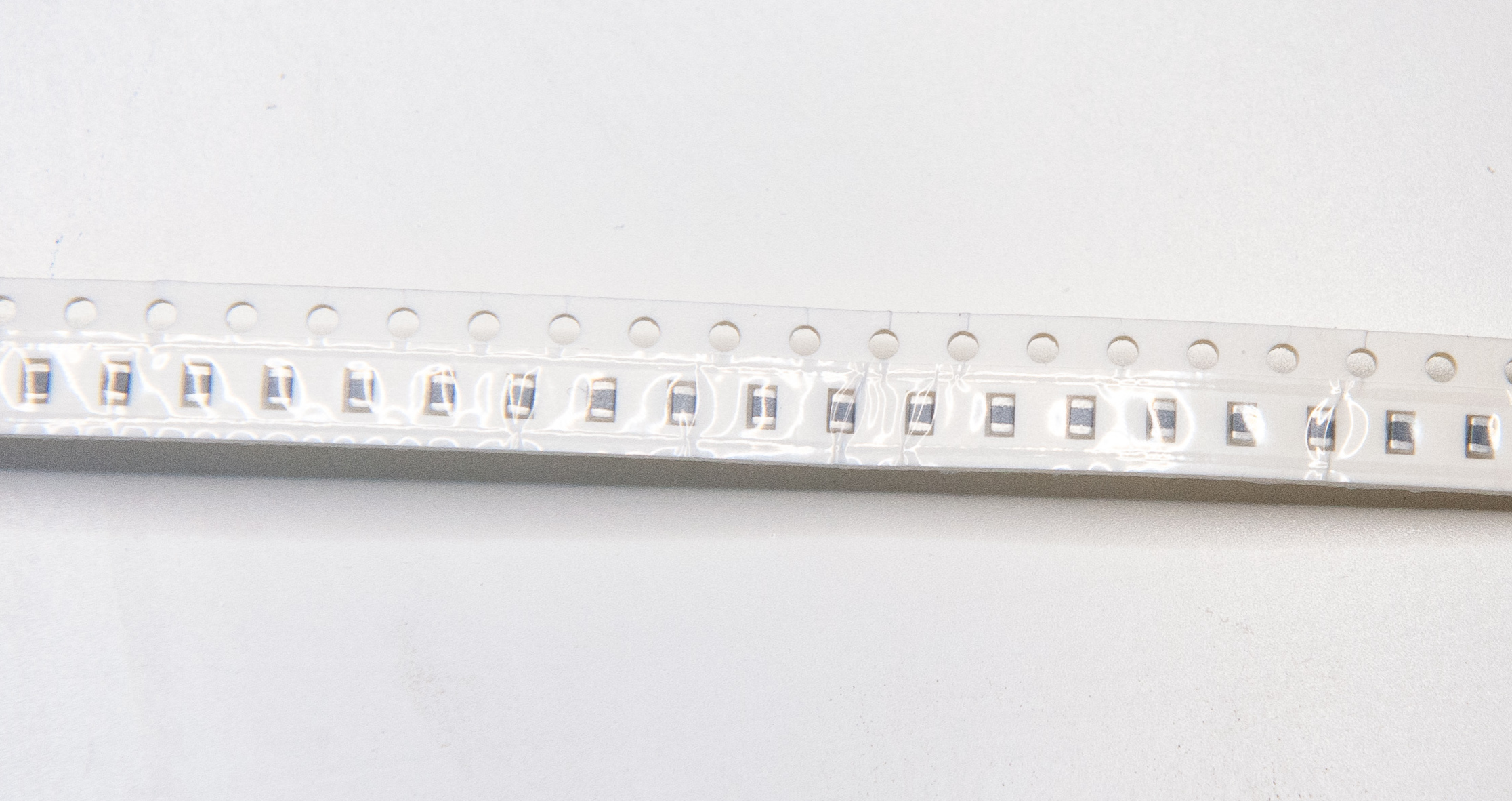
Those tapes are made of two parts: a small shiny transparent layer on the top (the cover tape) and the bottom the carrier tape. To get access to the component, you just need to peel off the top layer. Since those parts are very small, I recommend to keep them in their tape and peel off only the needed portion of the cover tape.
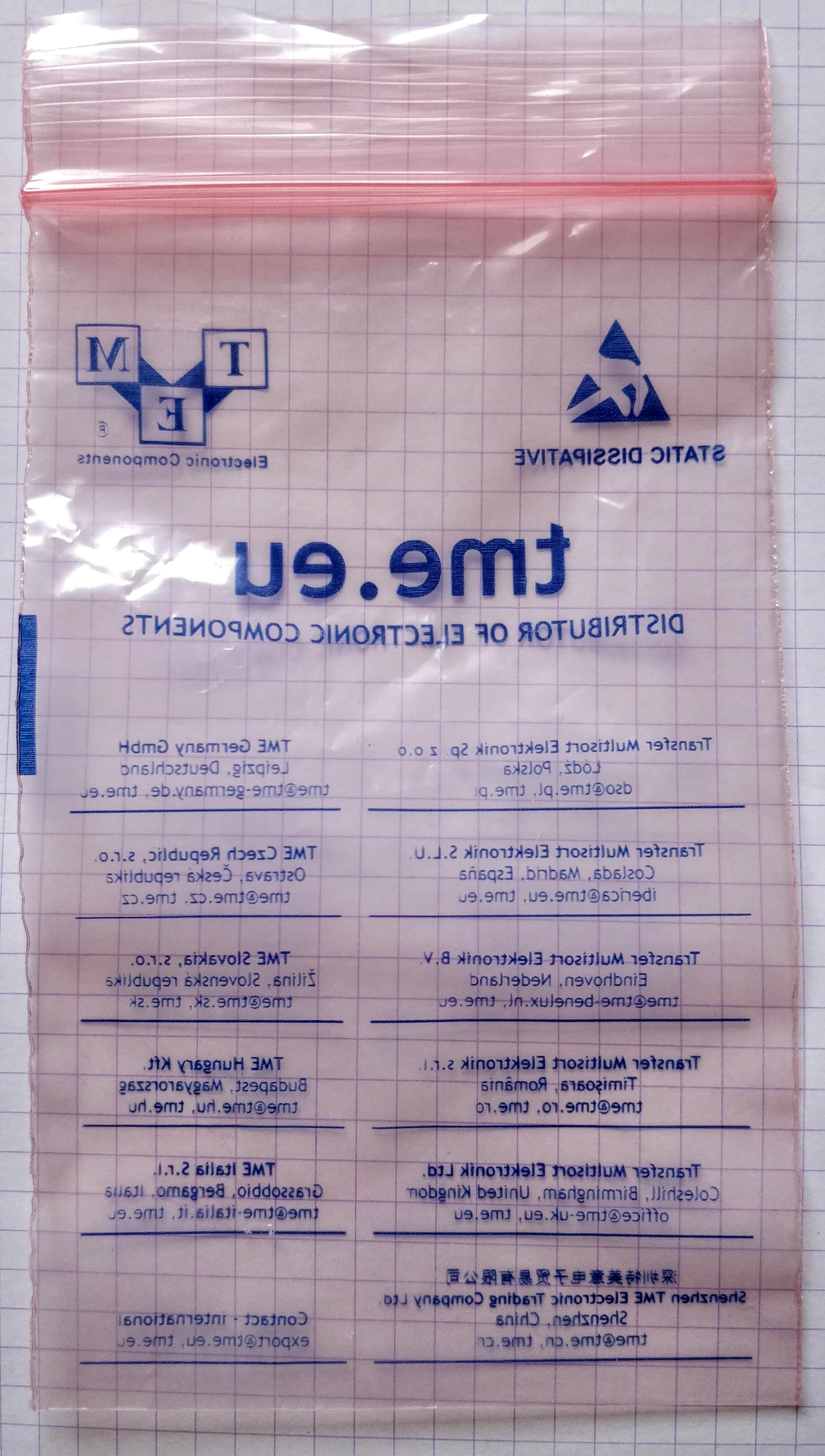
Components are sensible to electrostatic discharge (ESD), that’s why they’re shipped in special anti-static bags. There are two types of anti-static bags. The first kind is dissipative antistatic bags, usually made from polyethylene with a static dissipative coating. They work by dissipating the static charge that could build up on their surface onto other objects (including air) when the bag is touching something else. Those are usually red or pink:
The second kind is conductive antistatic bags, made with a conductive metal layer on top of a dielectric layer. Those bags protect their contents from ESD, because the metal layer forms a Faraday cage. You can recognize those bags because they are shiny and their color is gray or silver:
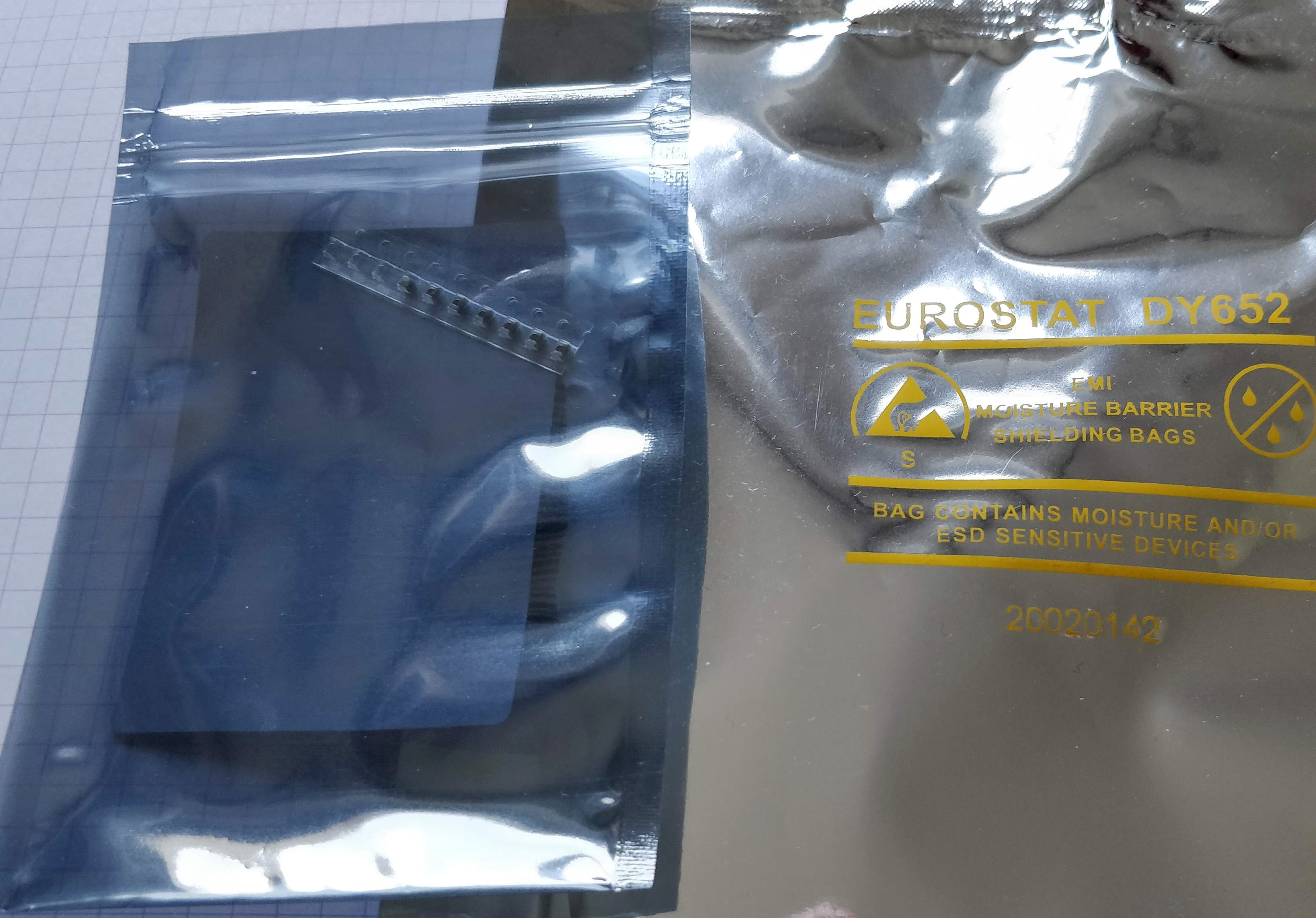
Note that those shielded bags are inefficient if the shield is not continuous, so make sure to not use bags with a perforation or puncture.
Components should always be stored in such bags, even for storage. Only remove the components from the bag when you’re ready to solder them on a PCB. And do so if possible in an anti-static environment (ie a specific table or mat is used).
Components should also be stored in a place that is not too humid. Some active components are shipped with desiccant bags inside the ESD protection bag, keep them when storing them as they absorb the excess humidity that could harm the part.
PCB assembly
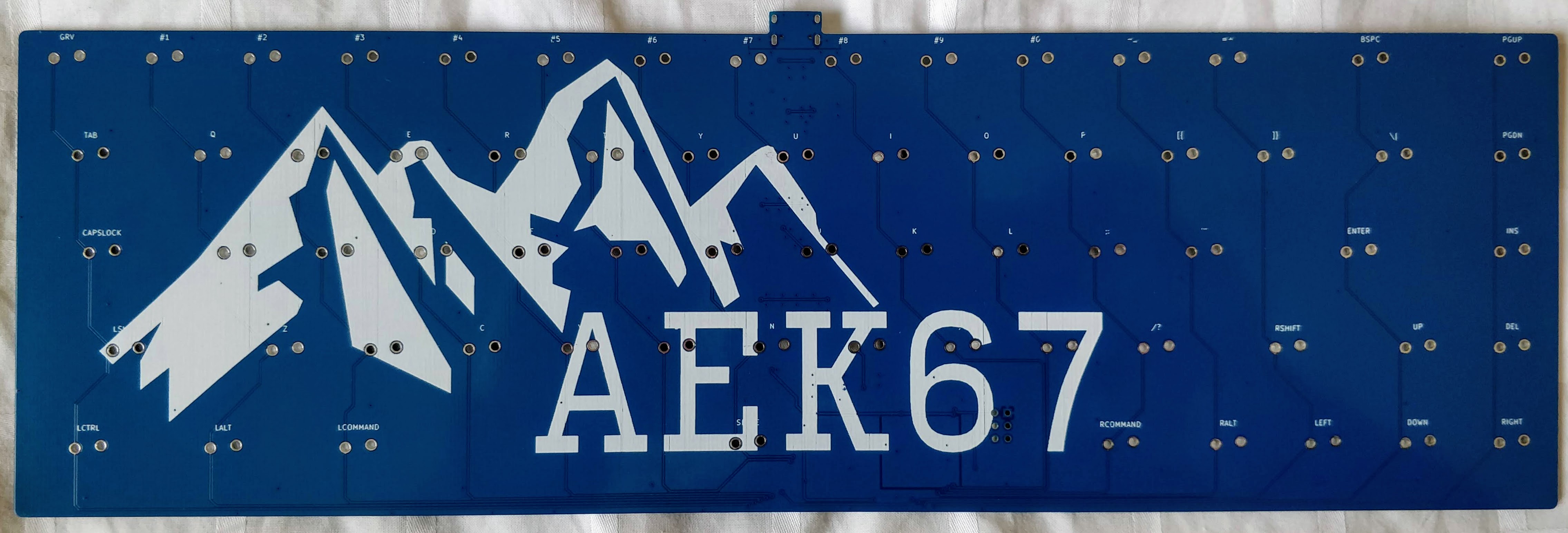
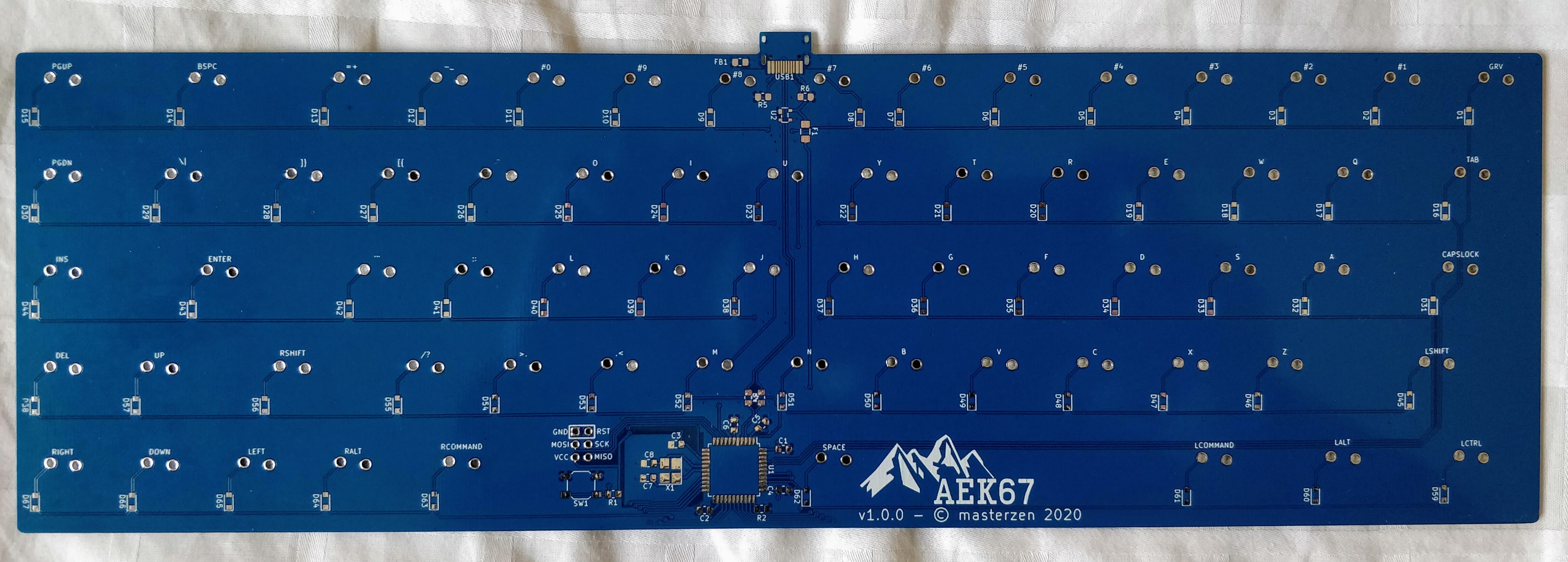
So, it’s mail day: I received the PCB:
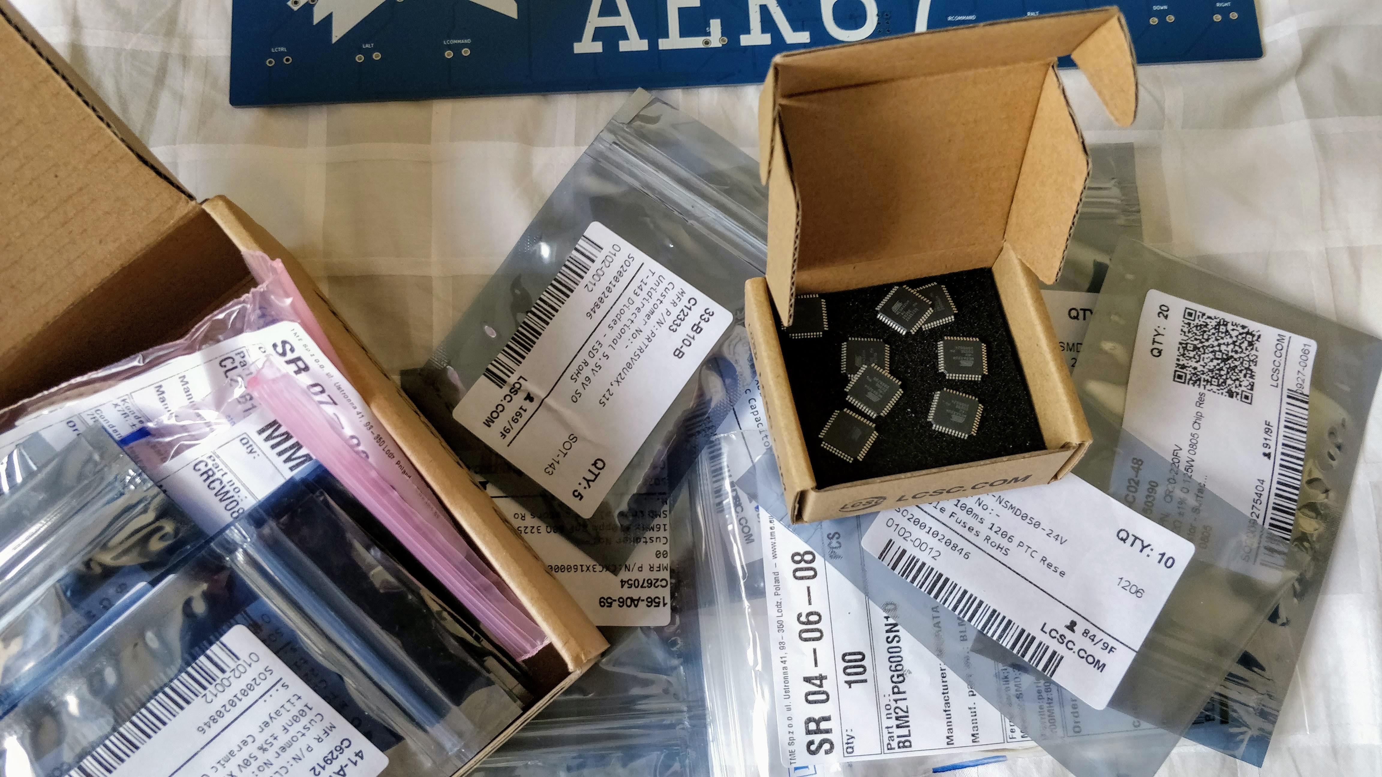
and the components (see the AtMega32U4 in the cardboard box in the center):
I’m now ready to assemble the PCB, that is solder all the components.
The tools
To do that the following tools are needed:
- ESD safe tweezers
- a soldering iron & tip
- tools to clean the iron
- solder
- extra flux
- desoldering tools
- magnifying tools
That’s the minimum required. Of course if you can afford a microscope or a binocular that would be awesome (I don’t have one, so that’s not strictly needed)
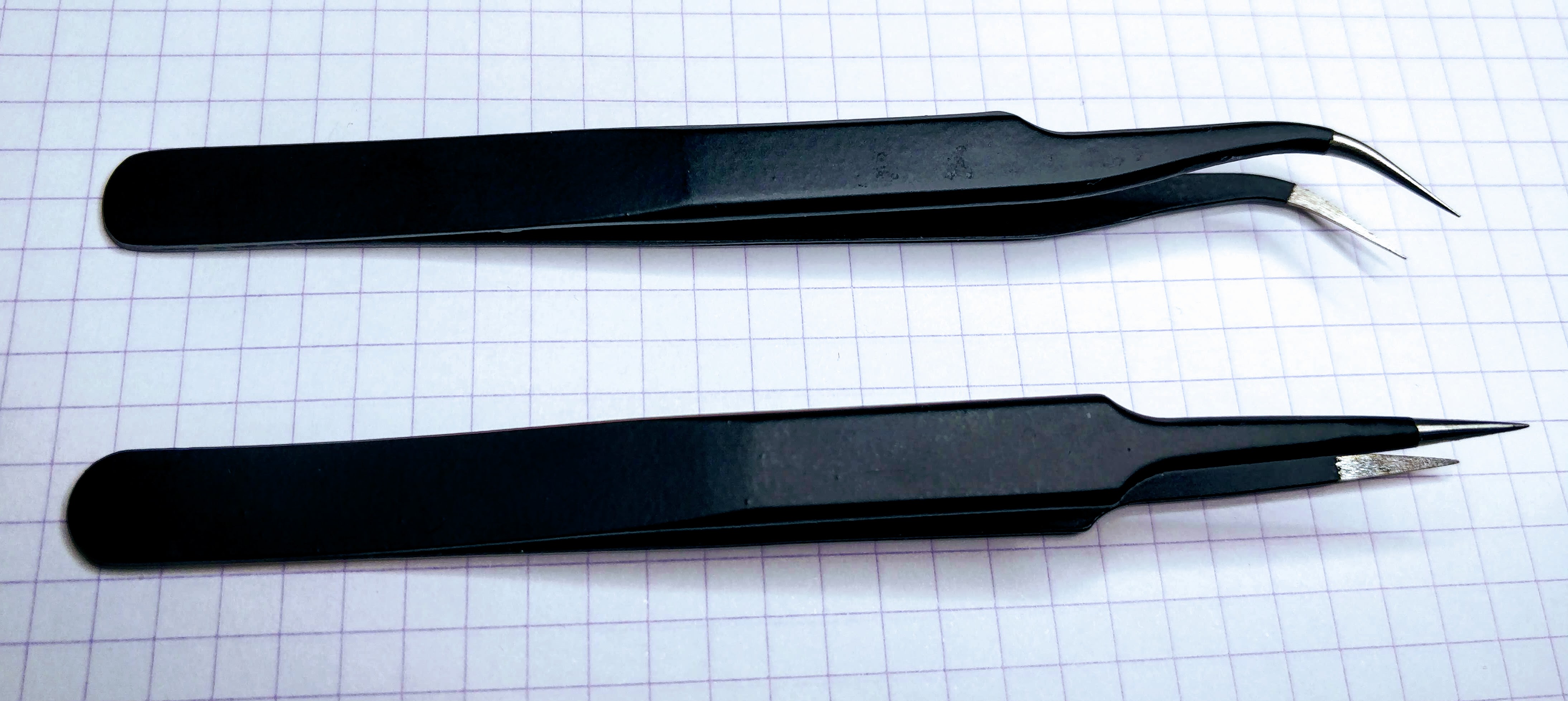
ESD tweezers
As I’ve explained earlier, electronic components can be destroyed by electro-static discharges. The human body is able to accumulate charges (for instance on walking on a carpet) and when touching another object discharge into it. Thus it’s important to prevent ESD when manipulating components.
To be able to place precisely the component on the PCB while soldering it, and also hold it while the solder solidifies, we need a pair of electronic tweezers. Since usually tweezers are made of metal, they would conduct the static charge to the component or the board. ESD tweezers are metallic tweezers that are coated with an non-conductive anti-static material, preventing the charges to be transferred from the body to the component.
You can find cheap tweezer sets at Amazon or more expensive ones at the previous vendors I cited for sourcing components.
Here are mine:
Soldering iron
I’ll recommend using a temperature controlled soldering iron, especially for soldering very small parts. One good choice would be either the Hakko FX888D, the FX951 or any other serious temperature controlled stations (among those made by Weller or Metcalf for instance). Hakko stations can be purchased in EU from batterfly.
You’ll also find Hakko T12 compatible stations on Aliexpress (like the KSGER T12), those are nice and inexpensive, unfortunately their PSU is rigged with defective designs that make them not as secure as they should (they probably wouldn’t pass CE conformity as is). I thus won’t recommend them (see this video for more information).
Then finally you can find standalone USB powered soldering irons like the TS80P or TS100. Those are very lightweight and have a custom opensource firmware superior to the original. They have a drawback: they’re not earthed by default and thus not completely ESD safe. The risk is a potential ESD destroying the SMD components that are being soldered. Regular wall-in soldering irons have the heating tip earthed and thus can’t build up an electrostatic charge. Moreover, those USB soldering iron are known to leak current when used. This can be fixed by adding an earth connection from the iron to common earth which requires a specific cable from the iron to an earth point (or at least a common potential point between you, the iron and the PCB, which can be done with specific anti-static workbench or mats). Some TS80P kits contain such earth grounding cables, some other not. I’m reluctant to recommand those for these reasons.
I myself have an inexpensive Velleman station (made in China). It’s certainly not the best, but it does its job reasonably well and is CE certified.
Rergarding soldering iron tips, you can find many different ones and it will depend on the soldering iron you’ve got. There are tons of different Hakko tips (here for the T12 tips). In this brand, the recommended ones for SMD parts are shapes D, BC/C and B. Regarding tip size, you can’t go wrong with D12 (or D16), B2 and BC2.
Iron tip cleaning
The soldering iron tip is critical for the tool performance. If it can’t perform its function of transferring heat to the solder joint, the soldering iron will not be efficient. Thus it is important to take care of the tip to prevent any soldering issues.
Soldering tips will wear throughout the time of use and will probably have to be replaced at some point. Careful tip hygiene will extend its life.
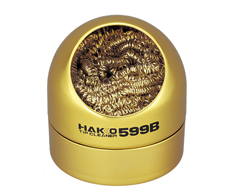
A particularly recommended tool is a metallic wool, like the Hakko 599b or a cheap clone:
Those cleaners are preferred other wet sponges, because the sponges will reduce the temperature of the iron tip when used, which means the tip will contract and expand quickly during cleaning. Frequent use of the sponge will cause metal fatigue and ultimately tip failure. Metallic wool cleaners are very effective at removing the dirt, contaminants, and flux or solder residues.
The idea is to prevent oxidation, for this, clean the tip before using the soldering iron on a new component, not after. While the tip is not used between two components, the flux and solder will protect the tip from oxidation.
When you’ve finished your soldering job, clean the tip with the metallic wool and tin the tip. It is possible to buy a tip tinning box. Most large solder manufacturer produce this kind of product, mine is this reference:

You might see recommandation of applying solder on the iron tip after use. This works fine if the solder contains a rosin activated flux (see below). But for no-clean solder (the majority of solder nowadays), the flux is not aggressive enough to remove or prevent tip oxidation. I recommend using a special tip tinner as the one above.
Solder
The solder is an alloy that melts from the heat of the iron to form the joint between the PCB pad and the component. It is important to purchase a good quality solder (especially if you have to perform some rework). There are two types of solder, those that contains lead and the lead-free variant. The latter is better for health and environment, but might be harder to use because it requires a higher soldering temperature. The former is easier to deal with, but is forbidden in EU because of RoHS compliance (it’s still possible to purchase leaded solder though).
Solder should also contain flux (even though as you’ll see later, adding flux is necessary to properly solder SMD components). The flux purpose is to clean the surfaces so that the solder wet correctly and adheres to the pad and components.
Solders are described by their content, like for instance Sn60Pb40, Sn63Pb37 or Sn96.5Ag3Cu0.5. It’s simply the percentage of their constituents. For instance Sn63Pb37 is an alloy made of 63% of tin and 37% of lead. Unleaded solder is mostly made of tin and silver, and sometimes a low level of copper.
For beginners, Sn63Pb37 would be the simplest solder to use. It is an eutectic alloy. This means that the alloy has a melting point lower than the melting point of any of its constituents (or any other variation mix of tin and lead), and that it has a very short solidifying phase. This makes this kind of solder easy to work with.
Unleaded solder have a higher melting point (around 220ºC) that might take time to be accustomed to.
Well, that doesn’t give you the temperature at which you’ll have to solder the components. For SMD parts, with leaded solder, I usually set my iron between 310ºC and 320ºC. This is high enough to quickly heat the pads. Lower temperature would mean to keep the iron tip longer on the pad and component with the risk of heating too much the component. Unlike common thought, the heat conductivity of metal decreases with temperature, which means that using a lower temperature would mean more heat accumulating in the component (because of the iron tip staying longer on the pad and component), and an increased risk of destroying it.
For unleaded solder, the recommended iron temperature is around 350ºC. But it also depends on the iron tip used. Smaller iron tips have a lower heat transfer surface and thus, you will need to use a larger temperature and longer soldering to achieve the same effect as with a larger tip.
Using a solder containing rosin flux is also recommended. The metallic surfaces in contact with air will oxidize, preventing the chemical reaction that will bond them to the solder during the soldering. Oxidization happens all of the time. However, it happens faster at higher temperatures (as when soldering). The flux cleans the metal surfaces and reacts with the oxide layer, leaving a surface primed for a good solder joint. The flux remains on the surface of the metal while you’re soldering, which prevents additional oxides from forming due to the high heat of the soldering process.
As with solder, there are several types of flux, each with their own key uses and limitations:
- Rosin (R): This is the most known one. It is a compound which was made originally from pine trees, but is now synthetic. Its liquefaction temperature is lower than the solder one, so it flows first. It becomes acid when liquified which allows its cleaning action before the solder melts to form the joint. The PCB needs to be cleaned after use with isopropyl alcohol (IPA) to remove residues.
- No Clean Flux (NC): It’s another big category. No-clean flux residue don’t need to be removed from the PCB. This flux should even be called “can’t clean” instead of no-clean, because if you want to remove residues, it’s very hard to do so and requires the proper solvent. The flux residues are usually transparent and non-conductive, so it’s fine to leave those on the board. Most solder nowadays contain NC flux.
- Rosin Mildly Activated flux (RMA): RMA is a compound made of rosin, solvents and a small amount of activator. RMA flux is not very aggressive and should be used with easily solderable surfaces (so it works well for SMD). The clear residue is normally non-corrosive and nonconductive. It might not be necessary to clean it after work.
- Rosin Activated flux (RA): Activity is higher than RMA, and should be used on oxidized surfaces. It is corrosive so it should be cleaned as soon as possible after work (with the appropriate solvent). The RA category also contains water soluble versions that also are highly corrosive, but can be cleaned with water (also because it’s conductive). Those are used to solder on difficult surfaces like stainless steel.
It’s still not finished about solder. How to choose the appropriate solder diameter? A good compromise for soldering a combination of SMD parts and through-hole components is 0.7 or 0.8mm.
Finally, soldering is a health hazard, so make sure to read the following important warnings:
- Make sure to wash your hands thoroughly after soldering.
- Solder in a ventilated room, do not inhale soldering smoke, purchase a fume absorber
- avoid eating, drinking, smoking in solder areas to prevent solder particulates to enter your body
Among the various brands of solder, those are known to produce good solder: MgChemicals, Kester, Weller, Stannol, Multicore, Felder, MBO etc. For a thorough comparison of several brands and models, you can watch SDG video: What’s the best solder for electronics
If you solder more than occasionally it might be worth investing in a small fume extractor like this Weller WSA350 or the Hakko FA-400.
Flux
The flux contained in the solder will not be enough to solder SMD parts. It is recommended to add extra flux before soldering the components, especially for ICs or fine pitch components (see below for the different techniques).
Flux exists in several forms:
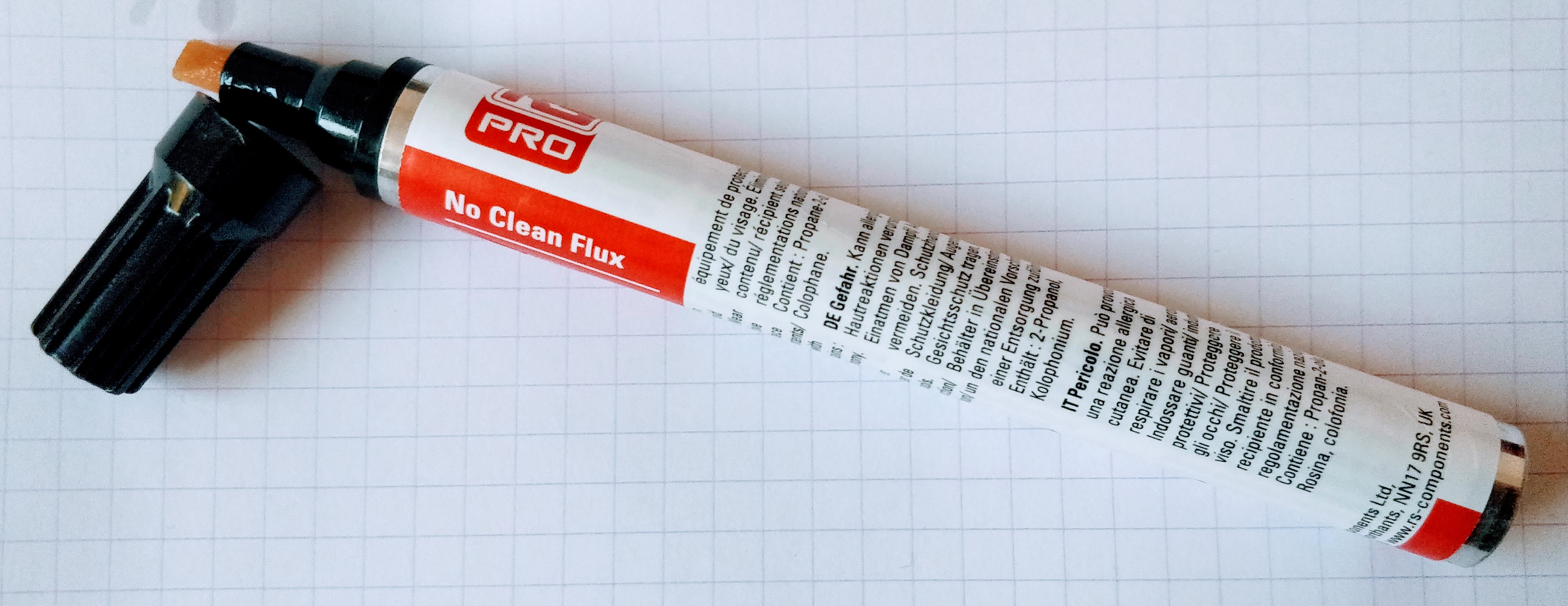
Here’s a flux pen:
And a flux serynge (ready to be used):
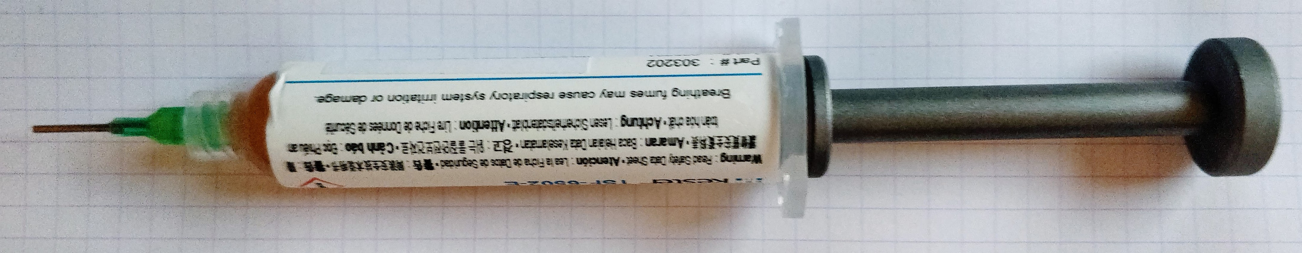
A note on flux serynge: most of them are sold without an applying nozzle and a plunger. That’s because professionals are using special dispensers. So do not forget to also purchase a plunger (they are dependent on the serynge volume) and nozzles. The nozzles are secured to the serynge by what is called a luer lock, which is a kind of threading inside the serynge.
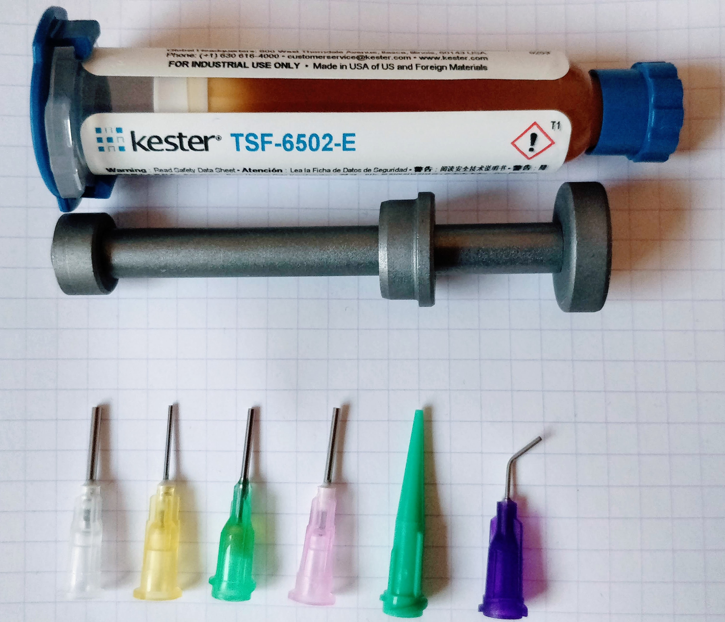
I recommend getting a flux paste serynge, as the flux from the pen is more liquid and tends to dry more quickly than the paste.
For a comparison of fluxes, you can watch the SDG video: what’s the best flux for soldering
Desoldering tools
Mistakes happens :) so better be ready to deal with them. It might be necessary to remove extra solder or remove a component misplaced by mistake. Without investing a lot of money in a desoldering iron or station, it is possible to get inexpensive tools that will help.
Let me introduce you to the desoldering pump and its friend the solder wick:
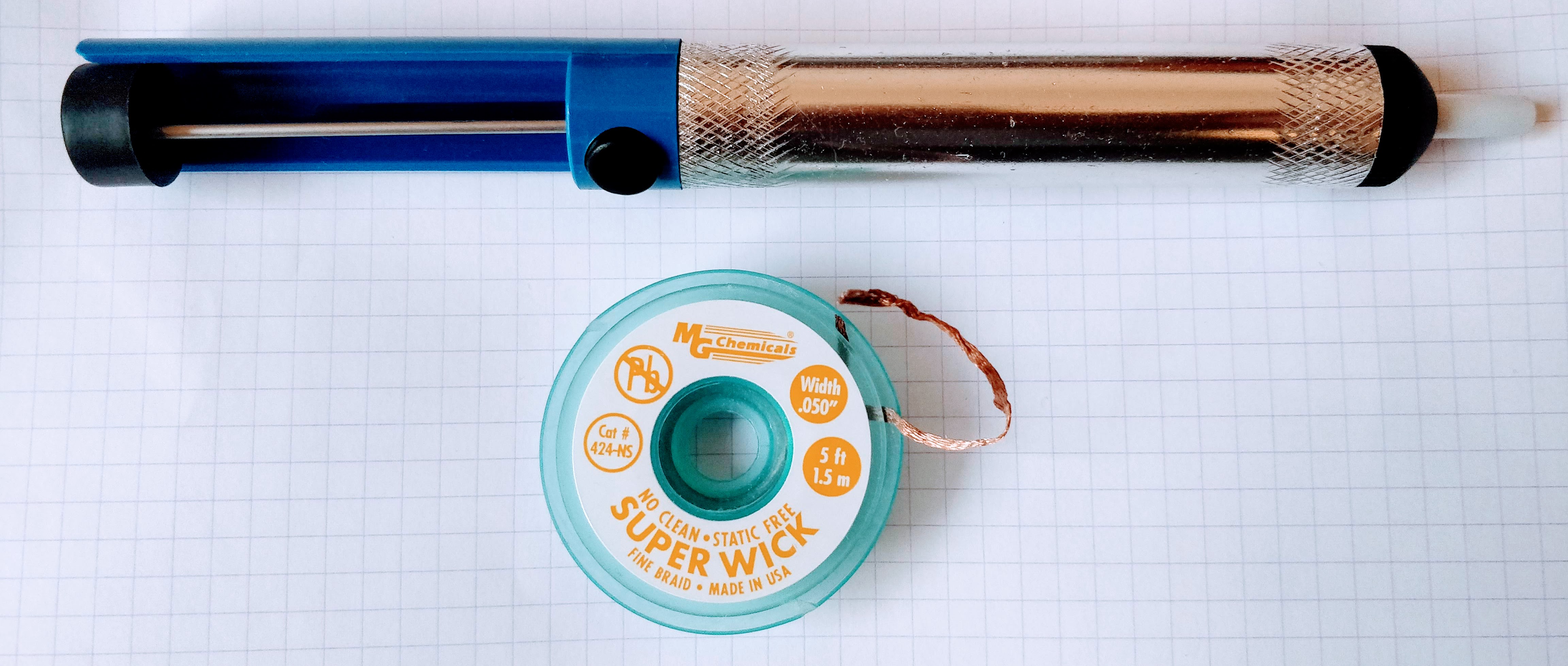
The top object in the picture is a desoldering pump. You arm it by pressing down the plunger. When released with the button, it will suck up the melted solder. It is to be used with the soldering iron heating the excess solder, then quickly apply the pump.
The solder wick is to be placed on the excess solder, then put the iron tip on top of it, the solder will melt and the wick will also suck it. It might be necessary to add a bit of flux before.
Magnifying tools
Finally the last tool needed when soldering small SMD parts is a good lamp with an integrated magnifier glass. As seen earlier, most of the component are less than 3 or 2 mm long, so it is hard to properly see them when soldering (unless you have very good eyes, which is not my case).
Of course getting a binocular or a microscope would be awesomely useful, but those are quite expensive (especially if you want quality). Instead I think a good magnifying glass lamp can do the job quite efficiently. The best ones are the Waldman Tevisio, unfortunately they are very expensive. It is possible to find cheaper alternatives on Amazon or one of the parts vendors I previously cited (I got myself this RS Online model).
The magnifying lens of such lamp is expressed in diopters. You can compute the magnifying ratio with the D/4+1 formula. A 5d lens will provide a 2.25x magnification. This is enough to solder small parts, but my experience (and bad eyes) show that when there’s a small defect its quite hard to have a good view of it (like when there’s a small bridge on two close pins on high-pitched ICs).
That’s why I also recommend getting a standalone small jewelry 10x magnifying glass. The Japanese Engineer SL-56 does an excellent work.
Assembling the PCB
Enough about the tools, let’s see how to assemble the components on the PCB. First let me explain how to solder SMD parts. The technique is the same for 2 pads or multiple pads, except for fine pitch ICs which will be covered afterwards.
I’m very sorry for the bad pictures and schemas that appears in the two next sections. I unfortunately don’t have a macro lens for my camera, and my drawing skills are, well, very low :)
Soldering techniques
2 pads component soldering technique
First apply a small amount of flux paste on both pads:
Next, wet a small amount of solder on one of the pad with the soldering iron:
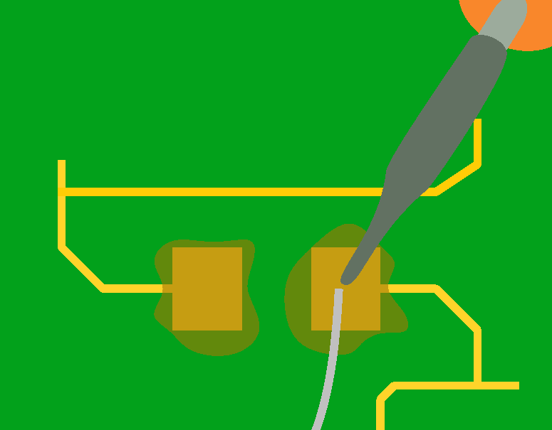
Then place the component with the tweezers, hold it firmly in place and reflow the solder on the pad until the joint is formed:
Once the solder has solidified, solder the other pad normally:
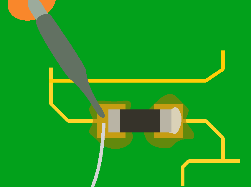
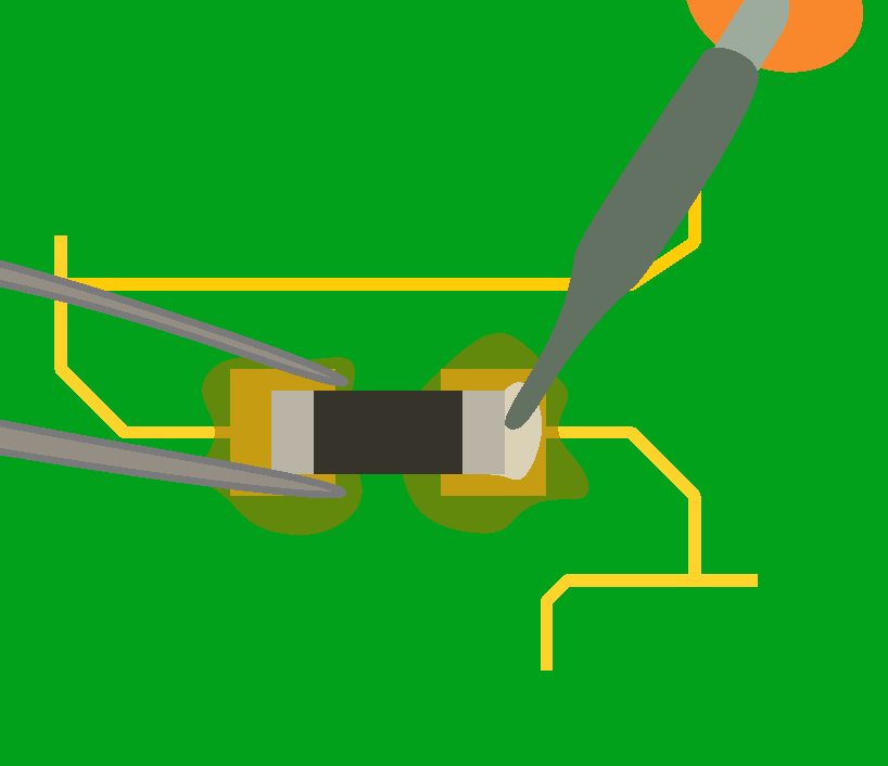
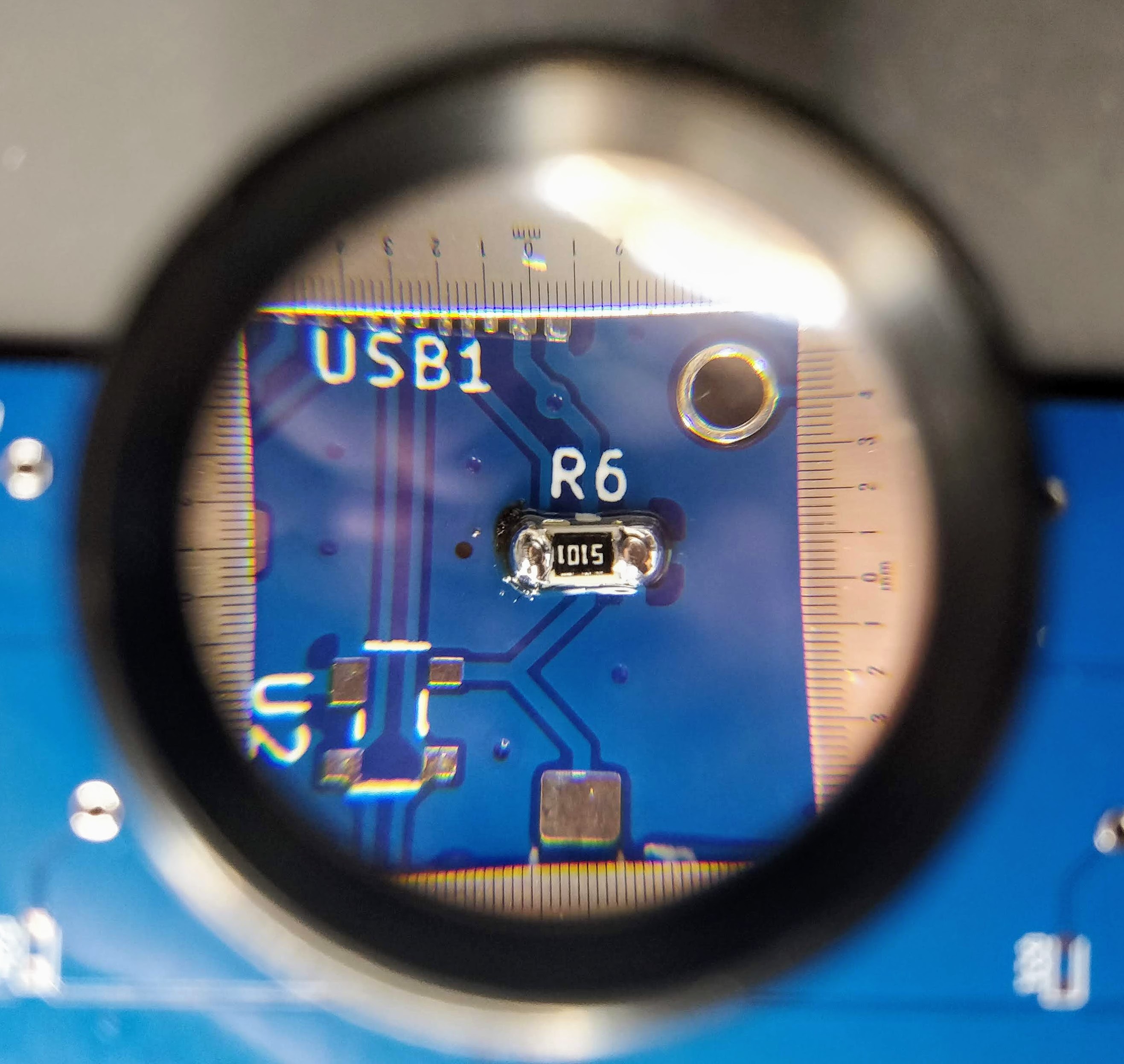
On a real component (here a 5.1k resistor near the USB receptacle), this give these steps:
Adding flux:
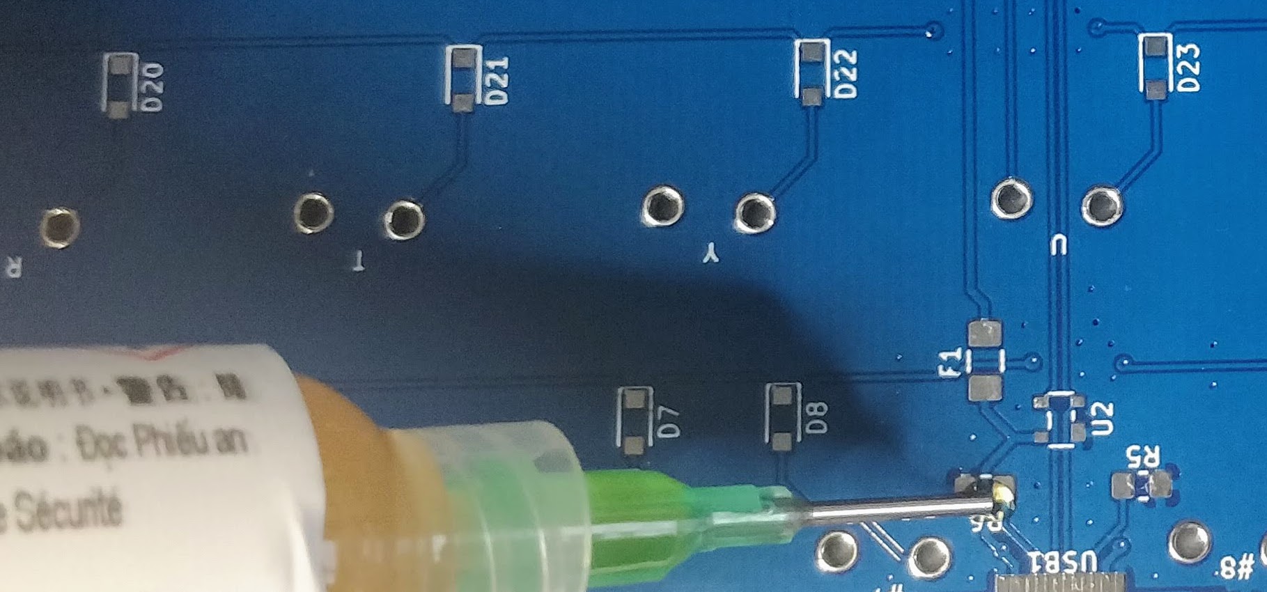
Apply some solder on one of the pad:
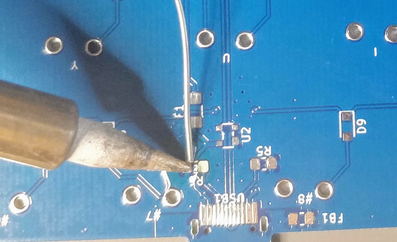
Place the component:

And since I don’t have three hands (and need one to take the picture), I soldered the first pad without holding the component (most of the time, when there’s enough flux the component will place itself correctly):
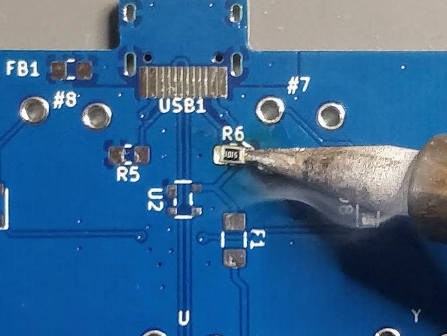
And the result (granted the component could be better aligned, the picture has been taken through the SL-56 magnifying glass):
This very same technique can also be applied to 3 or 4 legged components. Start by soldering one pin, making sure the component is correctly placed, then add solder on the other pins.
Drag soldering
The previous soldering technique doesn’t work for fine pitch components like ICs or the USB receptacle on this PCB. For this we need a different technique: drag soldering.
The drag soldering technique consists in first soldering 2 opposite pads of an IC, then to drag the soldering iron tip and solder along the pins relatively quickly. The flux and soldermask will do their job and solder will flow only on the metal parts. Bridges can happen if there’s too much solder or the iron tip is not moved quickly enough. That’s where the solder wick is useful to remove the excess solder.
To properly drag solder, first add solder on two opposite pads of the IC. Then carefully place the IC with the tweezers, hold it firmly and reflow those two pads (this is the same technique as for 2 pins components). When the solder solidifies and form a joint, the IC is secured at the right place, and we can start drag soldering.
Here’s a small schema illustrating the technique:
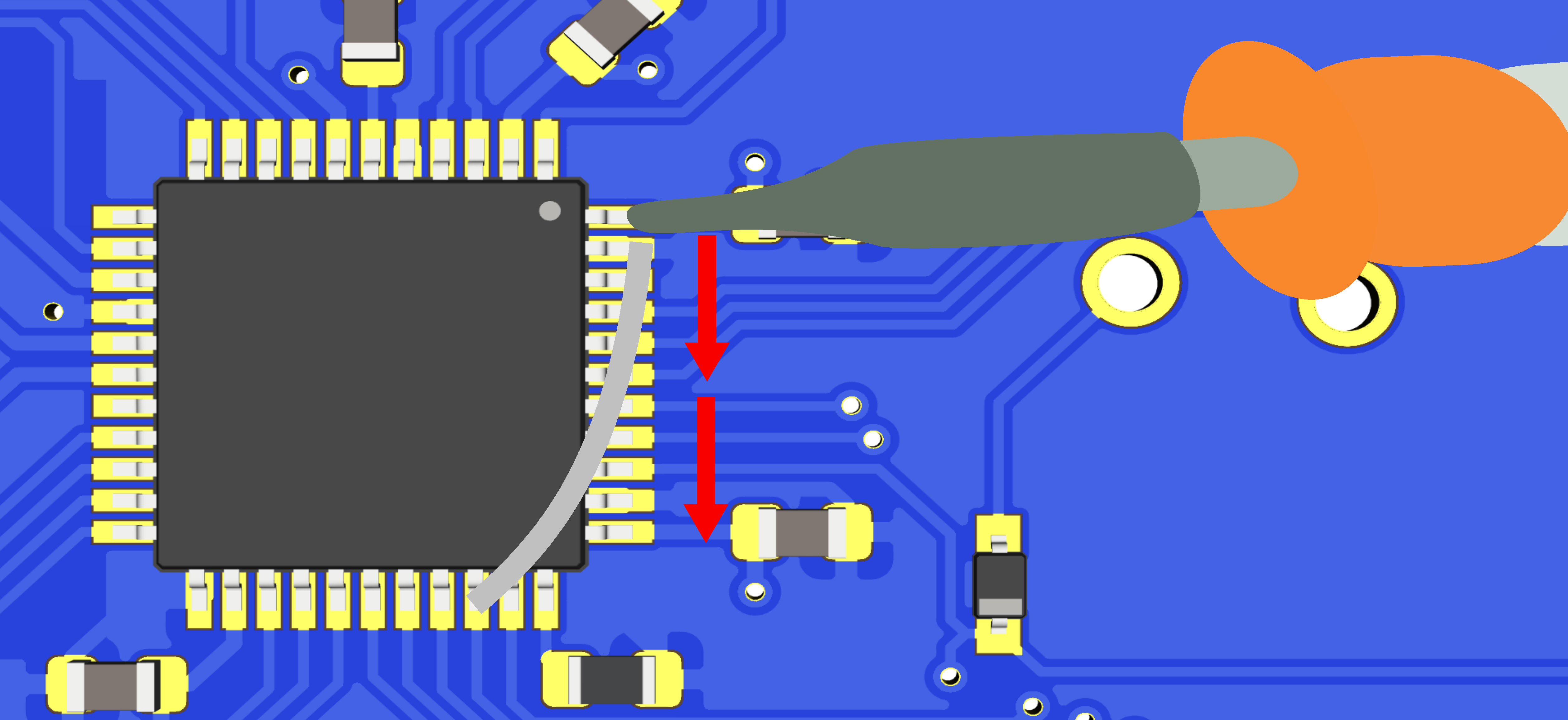
You’ll find the technique shown in this drag soldering video. Notice the tip shape used in the video (equivalent to a T12 BC), and how the solder is put under the tip. If you don’t use a slanted tip, you can still put some solder on the iron, or use what I described above, moving the solder at the same time as the iron tip.
Soldering the PCB
So I’m ready to solder the PCB with the aforementioned techniques. Since it’s harder to solder fine pitch components, it’s better to start with them. There’s nothing worst than soldering all 2-pads components, then failing soldering the most complex one and having to thrash the board.
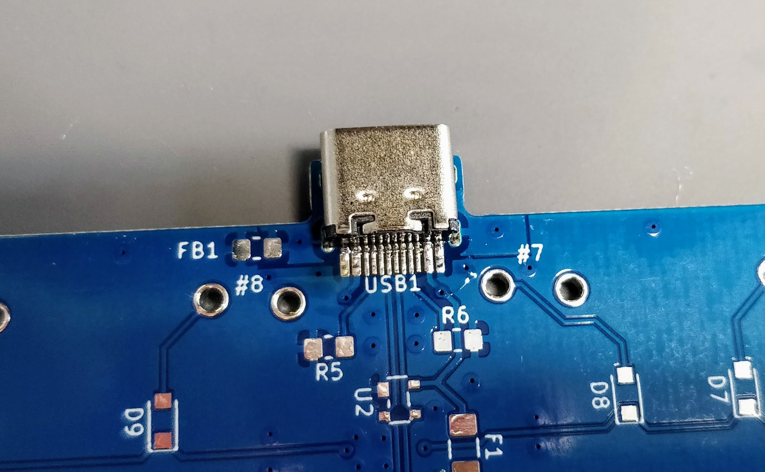
My advice is to start by soldering the USB connector first. Place it so that the small pins enter the board and solder on the front side. The USB connector is then now in place and the small pins are exactly placed on top of the pads on the back side of the PCB:
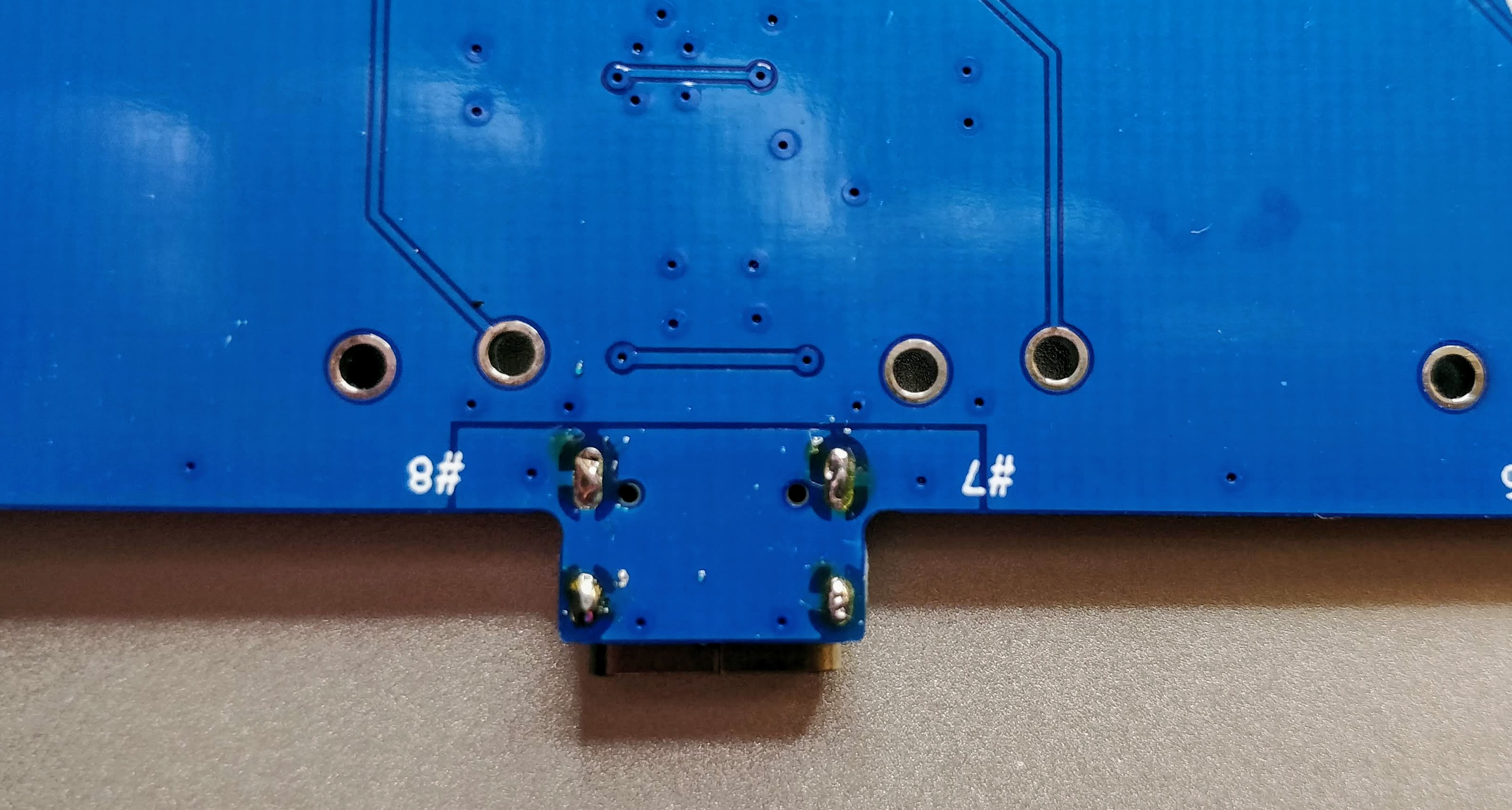
Then apply some flux paste on the other side accross the pins:
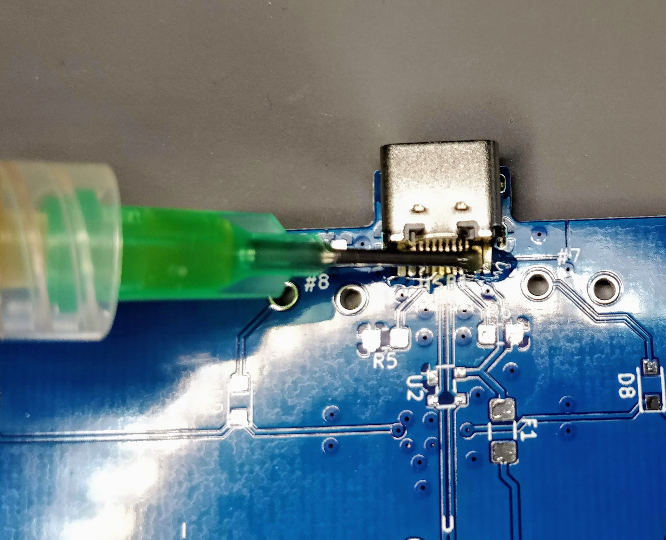
And drag solder the connector. This will give this (flux have been removed in the following picture):
Now is a good time to visually inspect there’s no bridge. Then it might also be a good idea to test that there’s no Vcc and GND short with a multimeter. Most multimeter (even the cheapest ones) have a “diode test” or continuity mode. In this mode the multimeter sends a very small current across the probes and measures the voltage. When the resistance is very small (if there’s electrical continuity between them) the multimeter will produce a beep. If there’s no continuity there won’t be any beep and the screen will show something specific (on mine it displays 1 which is very misleading).
With the multimeter in continuity testing mode, put the black probe on one of the GND pin and the other on one of the Vcc pin (or reverse, it doesn’t matter). There shouldn’t be any continuity (or beep). If there’s continuity, it means there’s a bridge that needs to be found and repaired by adding flux and using the iron tip or with the help of solder wick. You can test the other pins, there shouldn’t be any continuity except for pins that are doubled (D+/D-, GND, Vcc).
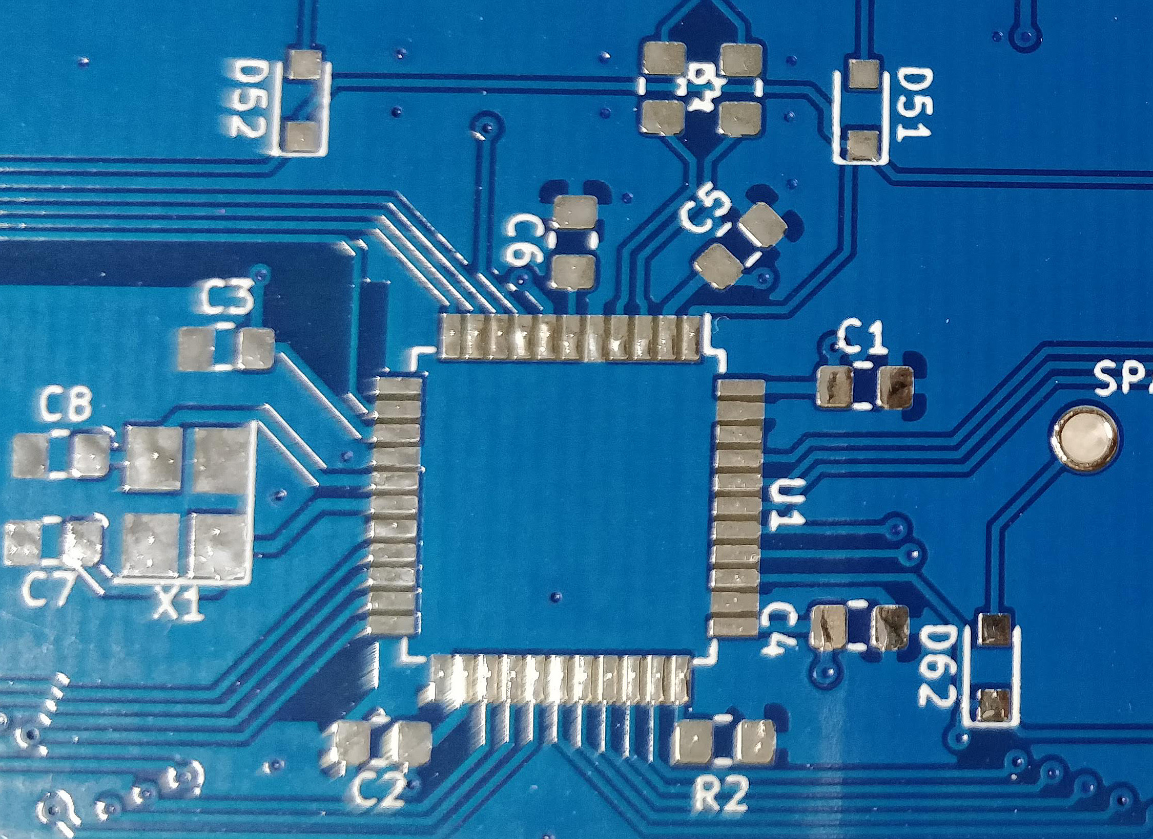
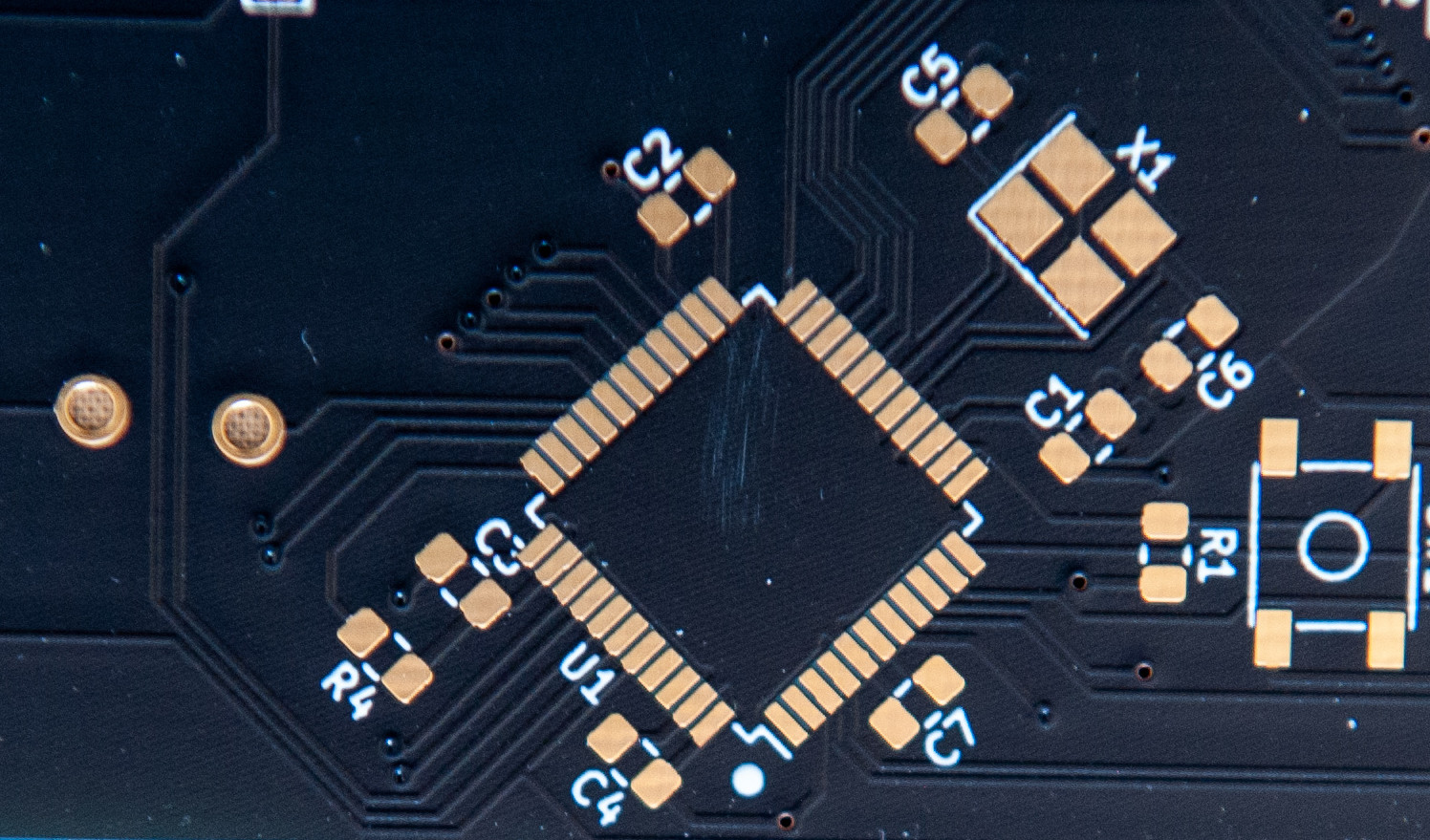
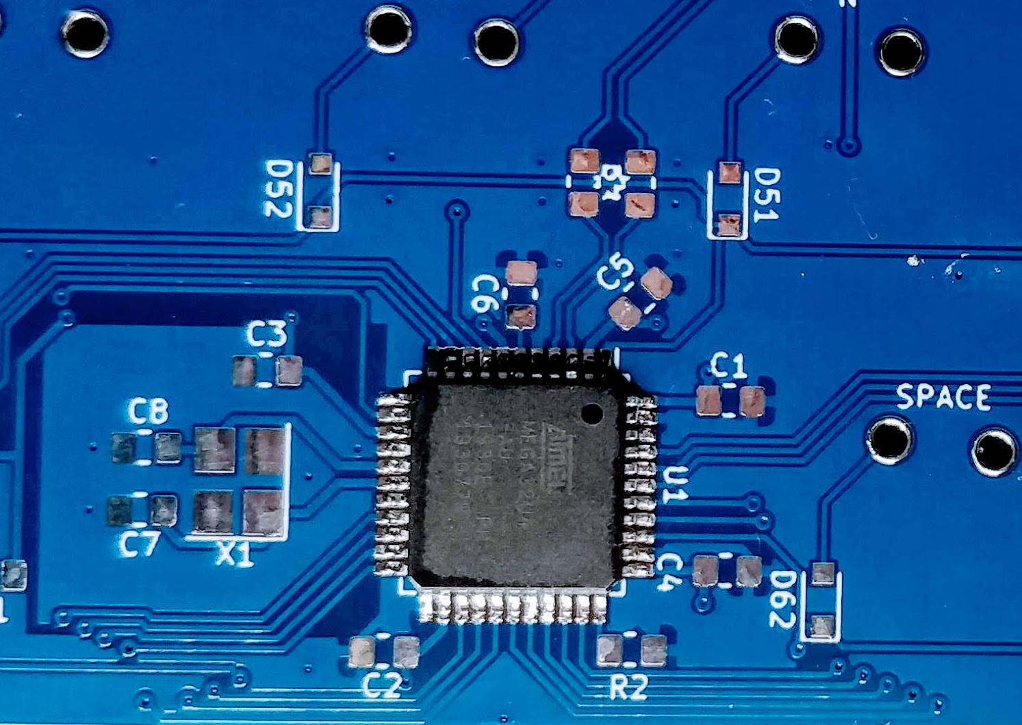
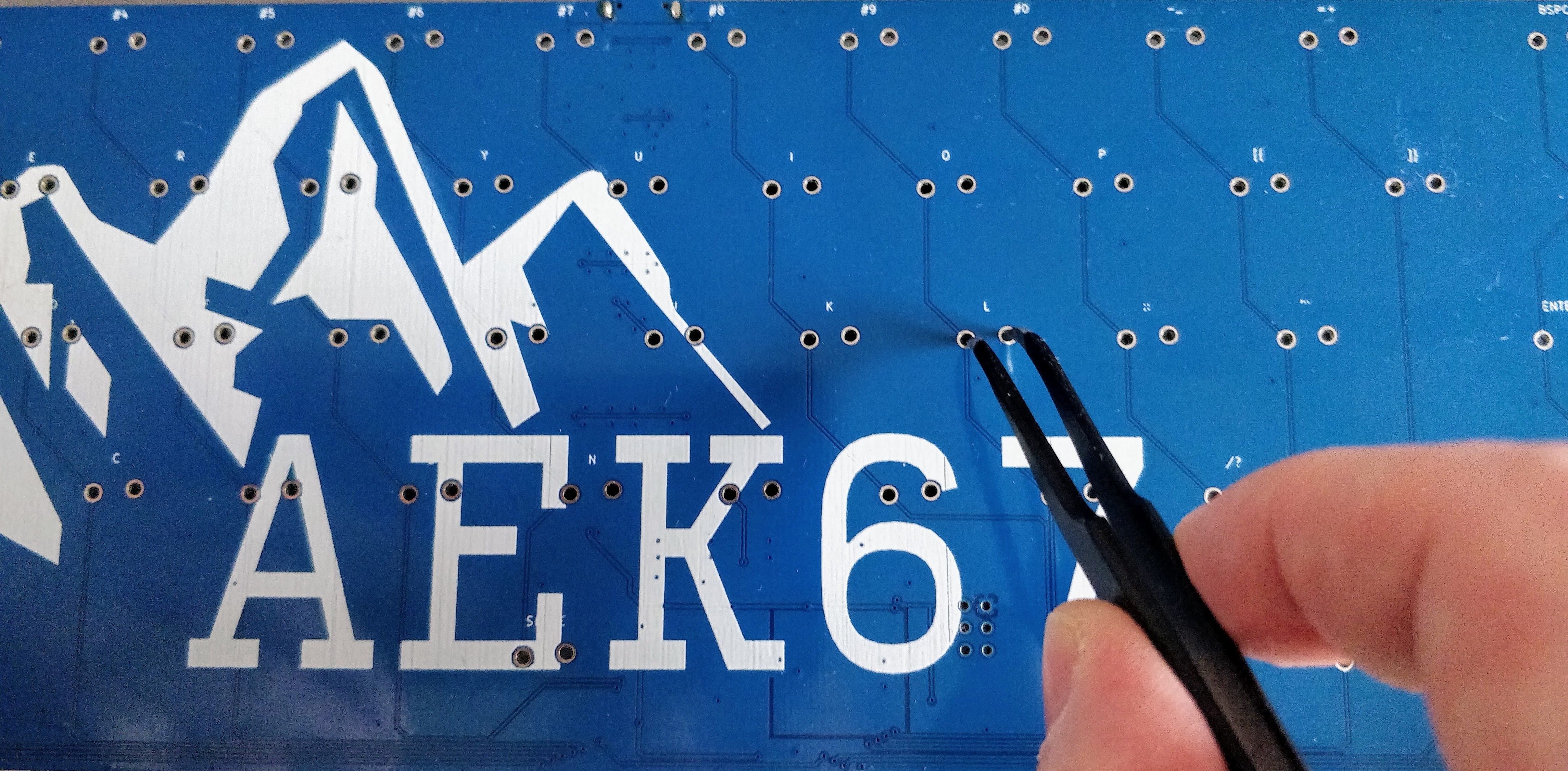
If everything is OK, the next step is to solder the AtMega32U4 MCU. First make sure to check how it should be placed. The silkscreen printed at the back of the board contains a small artifact indicating where pin 1 is. On the chip, the pin 1 is the pin close to the small point.
To make sure I’m soldering the component at the right place, I can use the Interactive HTML BOM plugin for Kicad. In the Kicad PCB editor, the plugin can be launched with Tools → External Plugins… → Generate Interactive HTML BOM. In the HTML Defaults section, it’s a good idea to select Highlight first pin and Layer View → Back only. After pressing Generate BOM, a web browser opens containing:
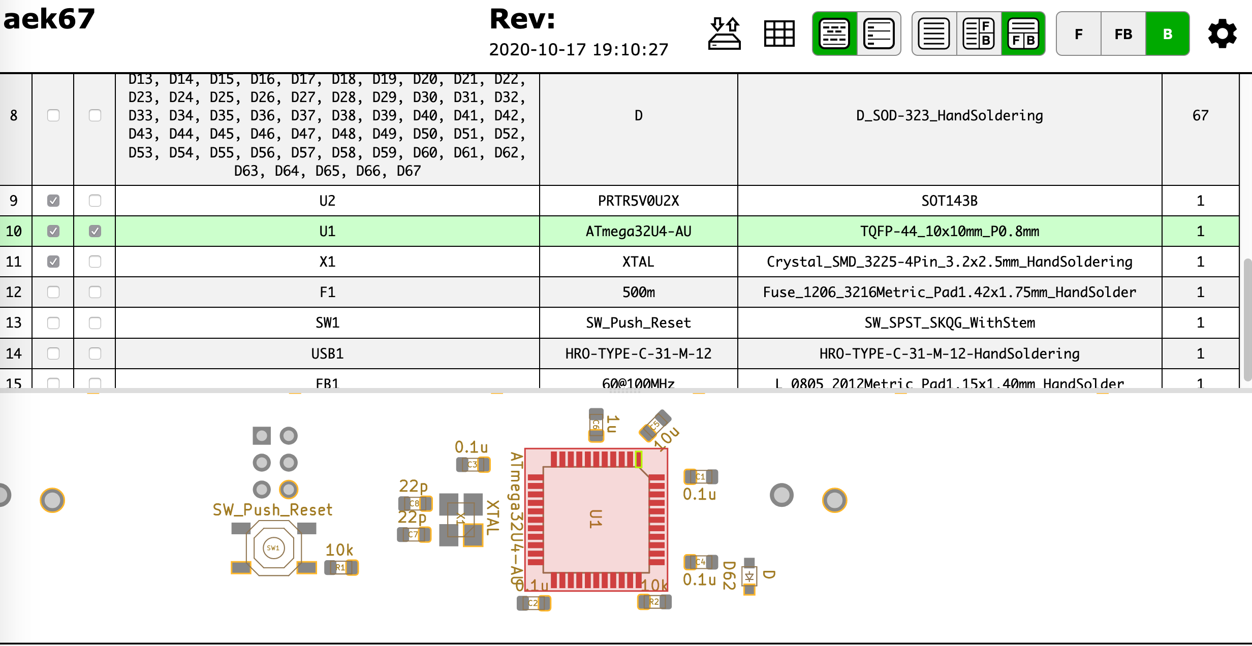
Notice that I selected the MCU. I can then see where the first pin is (it is outlined in flashy green), and how the MCU should be oriented.
So, I first add a bit of solder on pad 1 (top right in the picture) and another opposite pad:
Then I carefully place the MCU and reflow those pads to secure the MCU on the PCB (in the following picture it’s not that well placed, but I didn’t had a better picture):
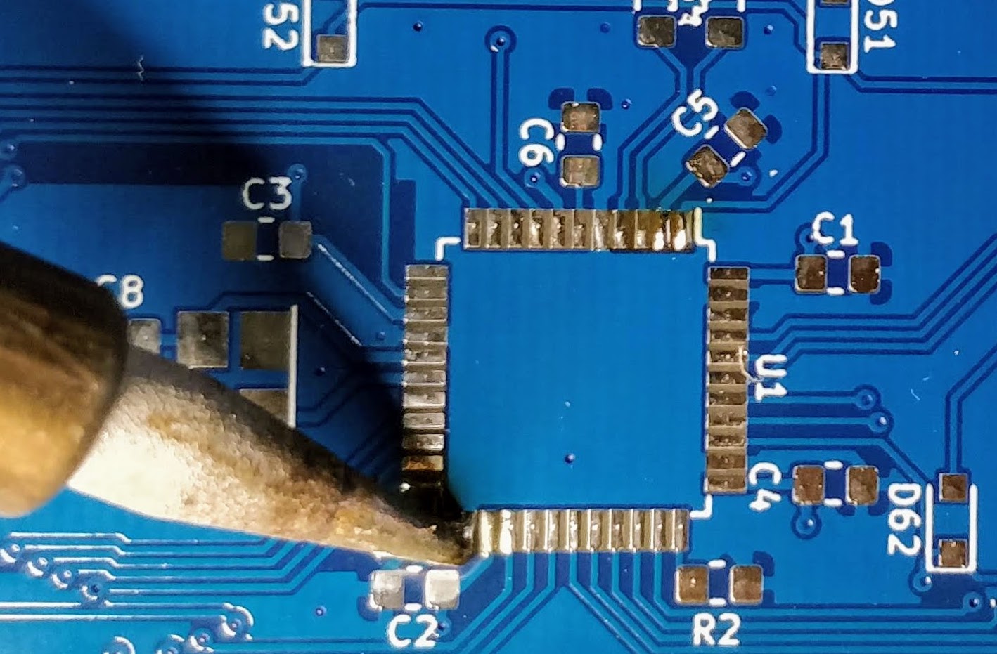
The next step is to add flux on the pins:
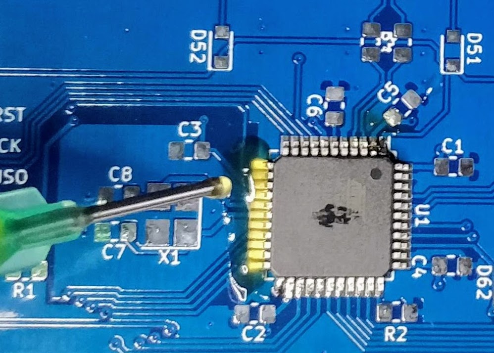
And drag soldering the left side:
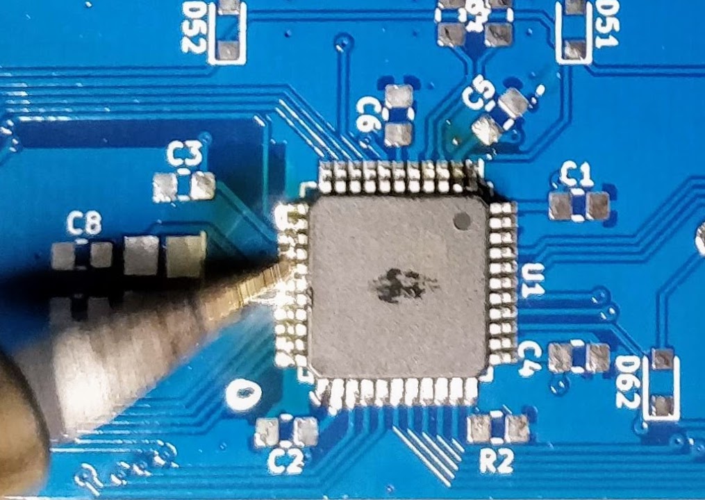
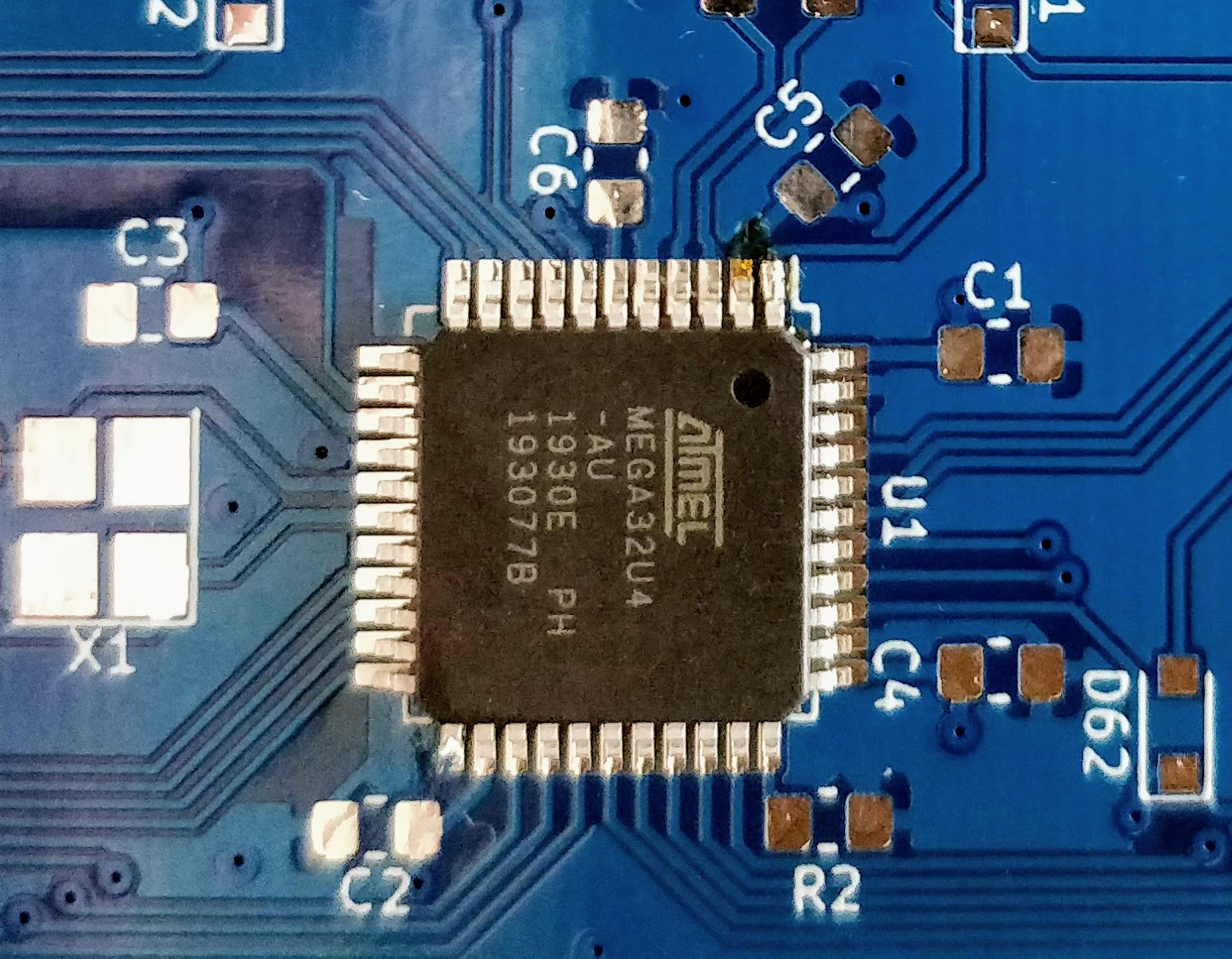
Repeat the operation on the other three sides. Here’s a picture after soldering the whole component, but before cleaning the flux residues:
And a visual inspection with the magnifying glass:
So what to solder next:
- the crystal oscillator: it’s relatively easy as the pads are gigantic compared to the component size. Note that this component is not polarized (even though there’s a slant in one of the pin, it just shows where pin 1 is).
- the PRTR5V0U2X and its four pins
- all decoupling capacitors close to the MCU
- all resistors
- the PTC fuse
F1 - the ferrite bead
- the reset switch
Do not solder the diodes yet. It’s long and tedious, so it’s better to test the MCU works correctly before soldering them.
An advice when soldering is to sort the component bags in the order of the component you want to solder (following the interactive HTML BOM for instance). It’s very hard when looking at SMD components to identity them. Most of the time there’s nothing written on them, or if there’s something it’s not very helpful. That’s why I recommend to open the bag of the component that will be soldered only at the moment of soldering them. So the ritual is:
- open the bag
- tear apart the band to release the exact number of needed components
- place them in a small recipient (so it’s convenient to get them with the tweezers).
- close the bag
- solder the components one by one
- move to the next ones
An alternative is to glue short sections of the components tapes on a cardboard board and tear apart the top tape when needed, then pick the components when ready to solder them.
Once all of the previously mentioned components have been soldered, it’s possible to test the PCB. Warning: do not connect yet the PCB to a computer. There could be a short circuit somewhere that could harm either the host or the keyboard (even though the host have some protections against those kind of failures).
Let’s see how to test the PCB with a multimeter. The first thing to check, is whether there’s continuity between the Vcc path, from the USB Vcc pins to the different MCU pins. If all Vcc pins are correct, check the GND pins. When all are correct, check there’s no continuity between GND and Vcc (at any point on the IC pins and USB pins). If that’s again fine, the next check is to make sure there’s no continuity between D+ and D- (this can be done at the USB connector).
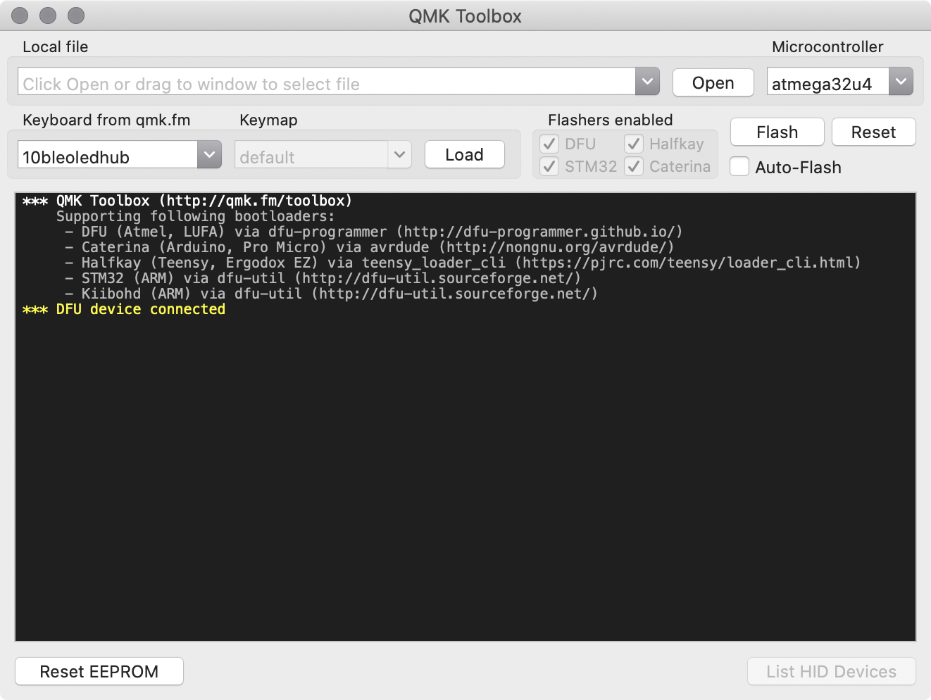
If everything is in oder, it is relatively safe to connect the PCB to a computer. Get an usb cable, then launch QMK toolbox. QMK Toolbox is a simple tool to help flashing QMK on a PCB. Once the keyboard is connected QMK Toolbox should display a yellow line indicating “DFU device connected” (at least for a DFU enabled MCU like our AtMega32U4):
If the test is conclusive, it’s time to solder the 67 diodes. Warning: diodes are polarized components, they need to be soldered with the correct orientation. A diode symbol looks like this:

One mnemotechnic way to remember which pin is what for a diode is to notice that the vertical bar and triangle form an inverted K and thus is the cathode, the triangle itself looks like an A (so is the anode).
On our schema and PCB, I’ve placed the cathode facing down:
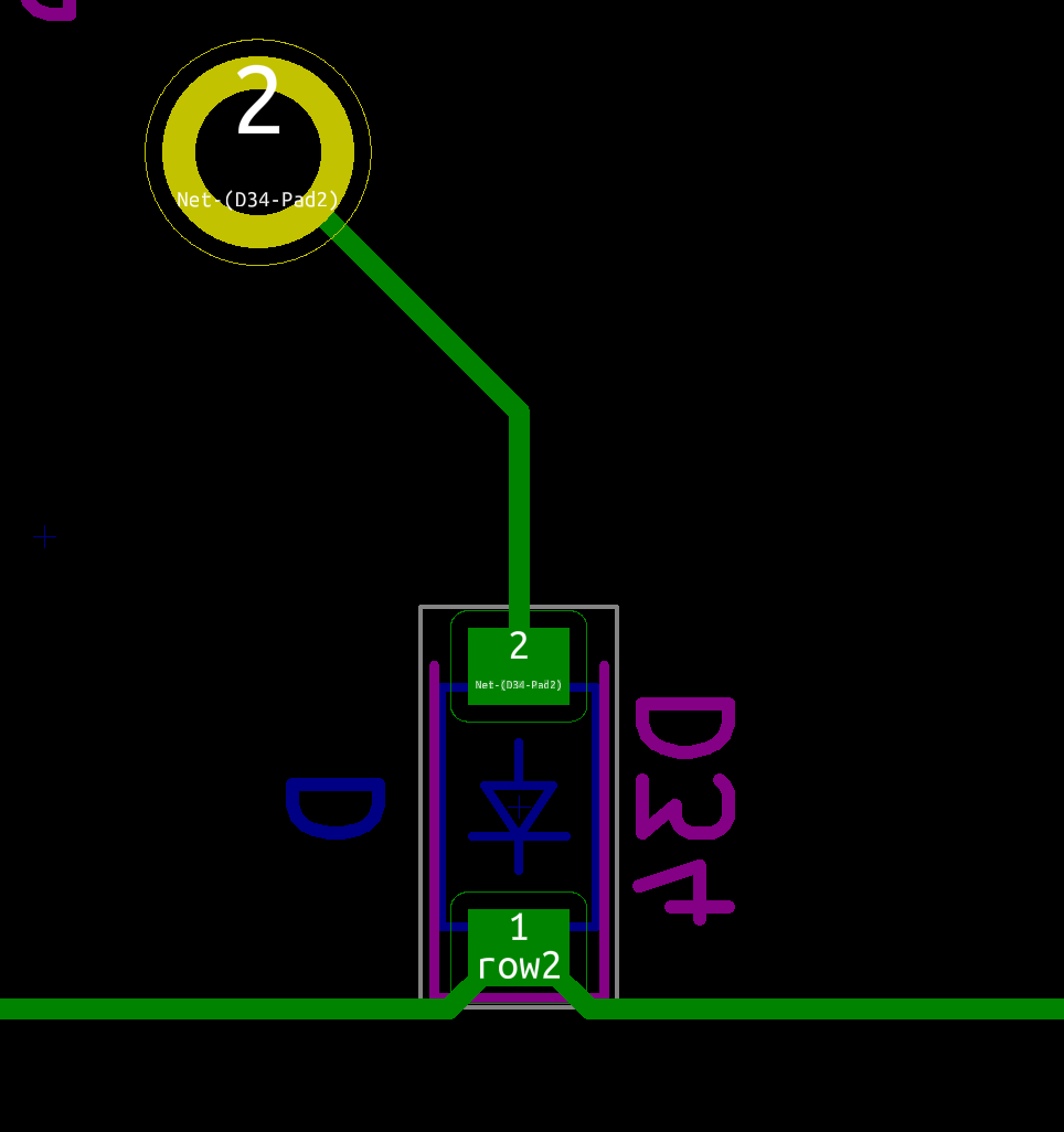
In Kicad, it’s easy to see the orientation of the diode because the B.Fab layer shows how to place it. On the manufactured PCB itself it’s not so easy as the fabrication layer is not shown. Instead we have a small horizontal bar to remind us where the cathode should be placed.
Hopefully the component itself also has a small bar printed on the top (here a close up of a 1N4148W-TP SOD-123, cathode on the left):
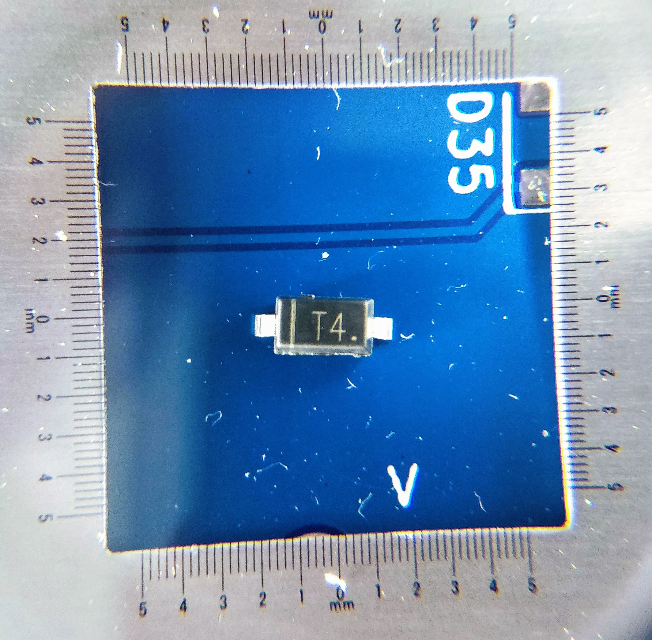
So to properly solder those diodes, it’s enough to align the component small bar with the bar printed on the PCB (which can partially be seen for the D35 diode in the image above).
The technique to solder a diode is the same as soldering any two pins SMD components. First add flux on both pads, add a small drop of solder on one of the pad, reflow it while holding the diode, then once solidified add a very small drop of solder on the other pad. Repeat for the 66 other diodes.
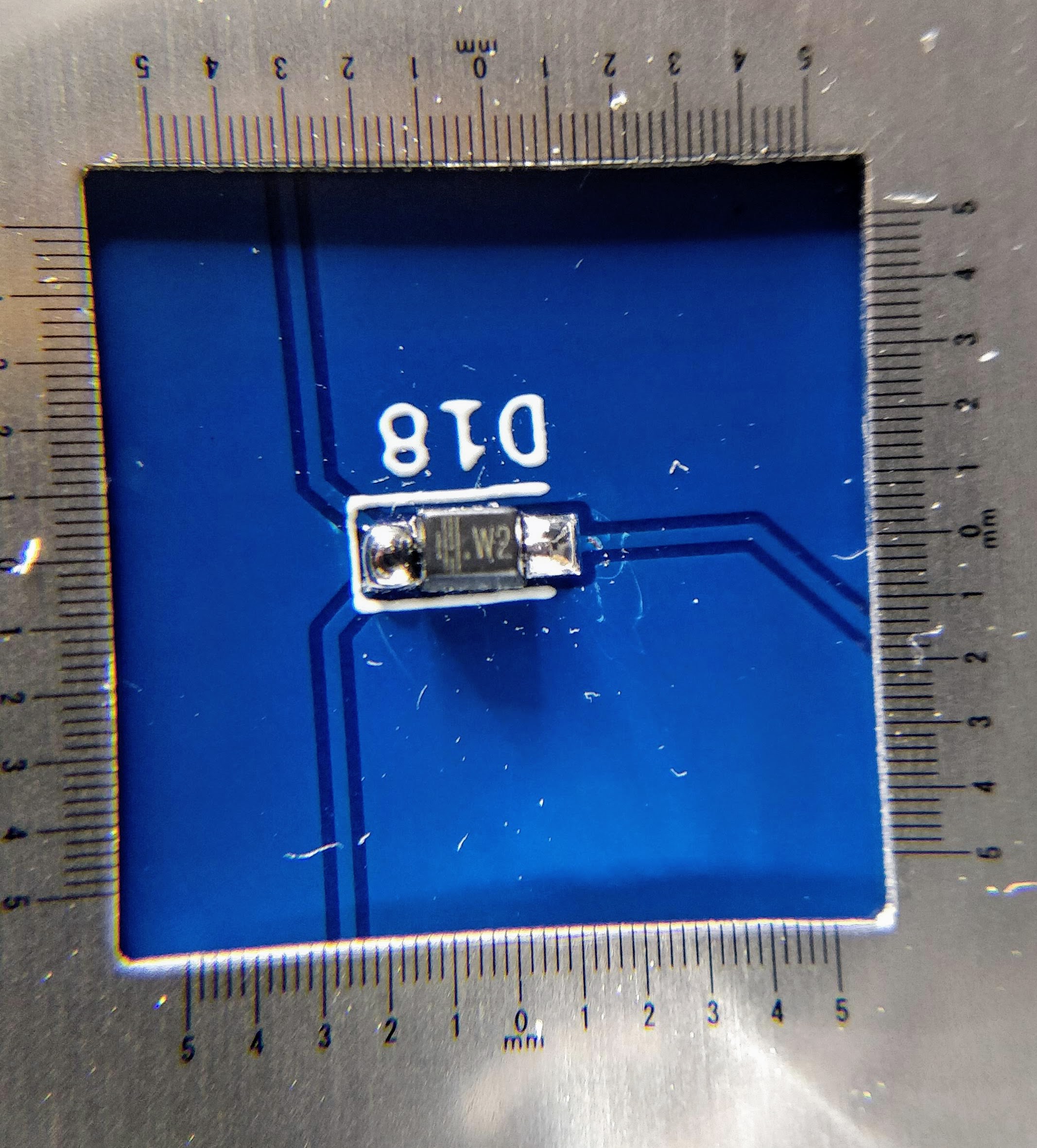
Here’s a soldered SOD-323 diode (smaller than the SOD-123 type we choose in this series of articles) :
Once all the diodes are soldered, we can also check with the multimeter that they’re correctly placed and soldered. Again, if I put the multimeter in “diode testing” mode, put the red probe on the switch pin connected to the diode and the black probe on the MCU pin where the row is connected, the multimeter should display a diode forward voltage drop (around 650 mV). If it doesn’t then either the diode is placed in the wrong orientation or there’s a joint issue (that’s how I detected that I had inverted the diode for the P key). If that happens, you need to visually inspect the diode and joints.
Programming the keyboard
To program the controller we’ll use QMK. This is an open source keyboard firmware forked and enhanced from TMK. It supports a miriad of custom keyboards and MCU (including various ATmega and ARM micro-controllers).
Follow QMK setup to install QMK and the needed toolchain on your computer.
Once done, check that you can compile a firmware, for instance the default DZ60 keymap:
% make dz60:default
QMK Firmware 0.11.1

Making dz60 with keymap default

avr-gcc (Homebrew AVR GCC 9.3.0) 9.3.0
Copyright (C) 2019 Free Software Foundation, Inc.
This is free software; see the source for copying conditions.  There is NO
warranty; not even for MERCHANTABILITY or FITNESS FOR A PARTICULAR PURPOSE.

Size before:
   text	   data	    bss	    dec	    hex	filename
      0	  23970	      0	  23970	   5da2	.build/dz60_default.hex

Compiling: keyboards/dz60/dz60.c                                                                    [OK]
Compiling: keyboards/dz60/keymaps/default/keymap.c                                                  [OK]
Compiling: quantum/quantum.c                                                                        [OK]
Compiling: quantum/led.c                                                                            [OK]
Compiling: quantum/keymap_common.c                                                                  [OK]
...
Compiling: lib/lufa/LUFA/Drivers/USB/Core/AVR8/USBController_AVR8.c                                 [OK]
Compiling: lib/lufa/LUFA/Drivers/USB/Core/AVR8/USBInterrupt_AVR8.c                                  [OK]
Compiling: lib/lufa/LUFA/Drivers/USB/Core/ConfigDescriptors.c                                       [OK]
Compiling: lib/lufa/LUFA/Drivers/USB/Core/DeviceStandardReq.c                                       [OK]
Compiling: lib/lufa/LUFA/Drivers/USB/Core/Events.c                                                  [OK]
Compiling: lib/lufa/LUFA/Drivers/USB/Core/HostStandardReq.c                                         [OK]
Compiling: lib/lufa/LUFA/Drivers/USB/Core/USBTask.c                                                 [OK]
Linking: .build/dz60_default.elf                                                                    [OK]
Creating load file for flashing: .build/dz60_default.hex                                            [OK]
Copying dz60_default.hex to qmk_firmware folder                                                     [OK]
Checking file size of dz60_default.hex                                                              [OK]
 * The firmware size is fine - 23816/28672 (83%, 4856 bytes free)
  5.37s user 4.17s system 82% cpu 11.514 total
You should obtain the dz60_default.hex file. You can remove it, it’s not needed.
QMK supports many keyboards and many layouts (called keymaps in QMK) for a given keyboard. A keyboard is defined by a directory in the keyboards/ folder, and each keymap is also a directory in the keymaps/ folder of a keyboard. To build such keymap, one need to use the make <project>:<keyboard>:<keymap> command.
The make command produces a hex file that can be flashed on the controller with QMK Toolbox, which is the recommended method. It is possible to flash from the command line depending on the controller bootloader type. I recommend QMK Toolbox because it is able to autodetect the correct bootloader, check the file size and so on. QMK Toolbox also acts as a console for the controller allowing to see debug statements.
Let’s bootstrap our new keyboard. Hopefully there’s a qmk command to do that:
% ./util/new_keyboard.sh
Generating a new QMK keyboard directory

Keyboard Name: masterzen/aek67
Keyboard Type [avr]:
Your Name: masterzen

Copying base template files... done
Copying avr template files... done
Renaming keyboard files... done
Replacing %YEAR% with 2020... done
Replacing %KEYBOARD% with aek67... done
Replacing %YOUR_NAME% with masterzen... done

Created a new keyboard called masterzen/aek67.

To start working on things, cd into keyboards/masterzen/aek67,
or open the directory in your favourite text editor.
This creates a set of files in keyboards/masterzen/aek67 that contains the default configuration for an AVR (ie AtMega) keyboard, including the default keymap:
% find keyboards/masterzen/aek67
keyboards/masterzen/aek67
keyboards/masterzen/aek67/aek67.h
keyboards/masterzen/aek67/config.h
keyboards/masterzen/aek67/keymaps
keyboards/masterzen/aek67/keymaps/default
keyboards/masterzen/aek67/keymaps/default/keymap.c
keyboards/masterzen/aek67/keymaps/default/readme.md
keyboards/masterzen/aek67/readme.md
keyboards/masterzen/aek67/aek67.c
keyboards/masterzen/aek67/info.json
keyboards/masterzen/aek67/rules.mk
I need to edit those files to map the hardware and matrix I created. Let’s start with the config.h file. This file contains the matrix description for this keyboard. We need to explain to QMK, what columns map to what pins on the MCU, and the orientation of the diodes. Based on our electronic schema, I can just write down the list of rows pins and columns pins:
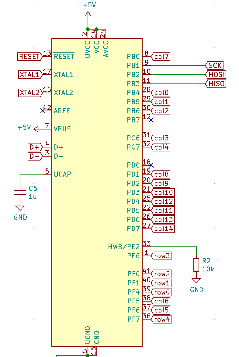
Here’s an extract of our config.h:
/* key matrix size */
#define MATRIX_ROWS 5
#define MATRIX_COLS 15

/*
 * Keyboard Matrix Assignments
 */
#define MATRIX_ROW_PINS { F4, F1, F0, E6, F7 }
#define MATRIX_COL_PINS { B4, B5, B6, C6, C7, F6, F5, B0, D1, D2, D3, D5, D4, D6, D7 }
#define UNUSED_PINS { B7, D0 }

/* COL2ROW, ROW2COL */
#define DIODE_DIRECTION COL2ROW
I defined here that the matrix is 5x15, and the ports of the rows and columns (in increasing order). Also, I tell QMK that the diodes are hooked between the columns and the rows (ie cathodes connected to the rows).
Next in rules.mk, we tell QMK everything about the controller used in this keyboard (there’s no need to edit anything there):
# MCU name
MCU = atmega32u4

# Bootloader selection
BOOTLOADER = atmel-dfu

# Build Options
#   change yes to no to disable
#
BOOTMAGIC_ENABLE = lite     # Virtual DIP switch configuration
MOUSEKEY_ENABLE = yes       # Mouse keys
EXTRAKEY_ENABLE = yes       # Audio control and System control
CONSOLE_ENABLE = no         # Console for debug
COMMAND_ENABLE = no         # Commands for debug and configuration
# Do not enable SLEEP_LED_ENABLE. it uses the same timer as BACKLIGHT_ENABLE
SLEEP_LED_ENABLE = no       # Breathing sleep LED during USB suspend
# if this doesn't work, see here: https://github.com/tmk/tmk_keyboard/wiki/FAQ#nkro-doesnt-work
NKRO_ENABLE = no            # USB Nkey Rollover
BACKLIGHT_ENABLE = no       # Enable keyboard backlight functionality
RGBLIGHT_ENABLE = no        # Enable keyboard RGB underglow
BLUETOOTH_ENABLE = no       # Enable Bluetooth
AUDIO_ENABLE = no           # Audio output
The next step is to define a key to matrix position mapping in aek67.h so that writing our keymap will be a bit easier:
...
#define LAYOUT_67_ansi( \
	K000, K001, K002, K003, K004, K005, K006, K007, K008, K009, K010, K011, K012, K013, K014, \
	K100, K101, K102, K103, K104, K105, K106, K107, K108, K109, K110, K111, K112, K113, K114, \
	K200, K201, K202, K203, K204, K205, K206, K207, K208, K209, K210, K211,       K213, K214, \
	K300, K301, K302, K303, K304, K305, K306, K307, K308, K309, K310,       K312, K313, K314, \
	K400, K401, K402,                   K406,                   K410, K411, K412, K413, K414  \
) { \
	{ K000,  K001,  K002,  K003,  K004,  K005,  K006,  K007,  K008,  K009,  K010,  K011,  K012,  K013,  K014 }, \
	{ K100,  K101,  K102,  K103,  K104,  K105,  K106,  K107,  K108,  K109,  K110,  K111,  K112,  K113,  K114 }, \
	{ K200,  K201,  K202,  K203,  K204,  K205,  K206,  K207,  K208,  K209,  K210,  K211,  KC_NO, K213,  K214 }, \
	{ K300,  K301,  K302,  K303,  K304,  K305,  K306,  K307,  K308,  K309,  K310,  KC_NO, K312,  K313,  K314 }, \
	{ K400,  K401,  K402,  KC_NO, KC_NO, KC_NO, K406,  KC_NO, KC_NO, KC_NO, K410,  K411,  K412,  K413,  K414 }  \
}
So the C macro LAYOUT_67_ansi contains 67 entries, one for each key, named by their rows and columns number (ie K204 is row2 and col4). This maps to a structure that represents the matrix in QMK (a double dimension array or rows and columns). Where the physical matrix has no switches (for instance in the bottom row before and after K406), we assign KC_NO so that QMK knows there’s nothing to be found there.
Next, let’s create the keymap. The keymap represents a mapping between the matrix switches and their functionality. When pressing a key, QMK will lookup in the keymap what keycode to send back to the computer. The computer will then interpret this keycode to a real character in function of the chosen layout. The keycode are defined by the USB HID standard. In QMK, they are defined as C macro whose name start with KC_. For instance KC_Q is the keycode for the Q key. See the QMK keycode table for an exhaustive list.
In QMK a keymap is a double dimension array of MATRIX_ROWS rows and MATRIX_COLS columns.
But that’s not the end of the story. QMK exposes different keymap layers. Layers are ways to assign multiple functions to a single key. We can assign a key in our keymap to switch to another layer where the keycode assigned is different than in the base layer. This is used for instance to map the function keys (F1 to F10) to the number keys.
Here’s the content of default/keymap.c:
enum layers {
    BASE,  // qwerty
    _FL,   // function key layer
};

/*
 * ,---------------------------------------------------------------------|
 * |`  |1  |2  |3  |4  |5  |6  |7  |8  |9  |0   |-   |=  |Backspace| PgUp|
 * |---------------------------------------------------------------------|
 * |Tab  |Q  |W  |E  |R  |T  |Y  |U  |I  |O  |P  |[  | ]  |   \     |PgDn|
 * |---------------------------------------------------------------------|
 * |Caps  |A  |S  |D  |F  |G  |H  |J  |K  |L  |;  |'  |  Enter     | Ins |
 * |---------------------------------------------------------------------|
 * |Shft    |Z  |X  |C  |V  |B  |N  |M  |,  |.  |/  |Shift       |Up| Del|
 * |---------------------------------------------------------------------|
 * |Ctrl|GUI |Alt |     Space                    |Alt |Fn  |  Lt |Dn |Rt |
 * `---------------------------------------------------------------------|'
 */
const uint16_t PROGMEM keymaps[][MATRIX_ROWS][MATRIX_COLS] = {
    [BASE] = LAYOUT_67_ansi(
        KC_ESC, KC_1,   KC_2,  KC_3,  KC_4,  KC_5,  KC_6,  KC_7,  KC_8,  KC_9,  KC_0,    KC_MINS,  KC_EQL,  KC_BSPC, KC_PGUP,
        KC_TAB, KC_Q,   KC_W,  KC_E,  KC_R,  KC_T,  KC_Y,  KC_U,  KC_I,  KC_O,  KC_P,    KC_LBRC,  KC_RBRC, KC_BSLS, KC_PGDN,
        KC_CAPS, KC_A,  KC_S,  KC_D,  KC_F,  KC_G,  KC_H,  KC_J,  KC_K,  KC_L,  KC_SCLN, KC_QUOT,           KC_ENT,  KC_INS,
        KC_LSFT, KC_Z,  KC_X,  KC_C,  KC_V,  KC_B,  KC_N,  KC_M, KC_COMM, KC_DOT,KC_SLSH,          KC_RSFT, KC_UP,   KC_DEL,
        KC_LCTL, KC_LGUI, KC_LALT,                  KC_SPC,                      KC_RALT, MO(_FL), KC_LEFT, KC_DOWN, KC_RGHT),

    [_FL] = LAYOUT_67_ansi(
        KC_GRV,  KC_F1, KC_F2, KC_F3, KC_F4, KC_F5, KC_F6, KC_F7, KC_F8,  KC_F9, KC_F10, KC_F11, KC_F12, KC_DEL, RESET,
        _______, _______, _______, _______, _______, _______, _______, _______, _______, _______, _______, _______, _______, _______, KC_HOME,
        _______, _______, _______, _______, _______, _______, _______, _______, _______, _______, _______, _______, _______, KC_END,
        _______, _______, _______, _______, _______, _______, _______, _______, _______, _______, _______, _______, KC_VOLU,_______,
        _______, _______, _______,                   _______,                            _______, MO(_FL), KC_BRID, KC_VOLD, KC_BRIU),
};
Notice a few things:
- I’m using the
LAYOUT_67_ansimacro that I defined inaek67.h. This is to simplify using the matrix, because the matrix doesn’t have all the switches implemented. - there are two layers, the base one called
BASEand the so-called function layer_FL, that contains a few more keys. - the
_______is an alias forKC_TRANSwhich means that this key isn’t defined in this layer. When pressing this key while being in this layer, the keycode that will be emitted is the first one to not beKC_TRANSin the layer stack. That means thatEnterfor instance is stillEntereven for the_FLlayer, but the up arrow key is volume up in the_FLlayer. - I’m including a
RESETkey, so that it is easy to enter DFU mode to flash the keyboard (no need to open the case to get access to the hardware reset button) MO(_FL)is a special keycode that tells QMK to momentary switch to the_FLlayer as long as the key id pressed. So activatingRESETmeans maintainingMO(_FL)key and pressing the Page up key.
Now let’s build the firmware:
% make masterzen/aek67:default
QMK Firmware 0.11.1

Making masterzen/aek67 with keymap default

avr-gcc (Homebrew AVR GCC 9.3.0) 9.3.0
Copyright (C) 2019 Free Software Foundation, Inc.
This is free software; see the source for copying conditions.  There is NO
warranty; not even for MERCHANTABILITY or FITNESS FOR A PARTICULAR PURPOSE.

Size before:
   text	   data	    bss	    dec	    hex	filename
      0	  18590	      0	  18590	   489e	.build/masterzen_aek67_default.hex

Compiling: keyboards/masterzen/aek67/aek67.c                                                        [OK]
Compiling: keyboards/masterzen/aek67/keymaps/default/keymap.c                                       [OK]
Compiling: quantum/quantum.c                                                                        [OK]
Compiling: quantum/led.c                                                                            [OK]
Compiling: quantum/keymap_common.c                                                                  [OK]
Compiling: quantum/keycode_config.c                                                                 [OK]
Compiling: quantum/matrix_common.c                                                                  [OK]
Compiling: quantum/matrix.c                                                                         [OK]
Compiling: quantum/debounce/sym_defer_g.c                                                           [OK]
...
Compiling: lib/lufa/LUFA/Drivers/USB/Core/AVR8/USBController_AVR8.c                                 [OK]
Compiling: lib/lufa/LUFA/Drivers/USB/Core/AVR8/USBInterrupt_AVR8.c                                  [OK]
Compiling: lib/lufa/LUFA/Drivers/USB/Core/ConfigDescriptors.c                                       [OK]
Compiling: lib/lufa/LUFA/Drivers/USB/Core/DeviceStandardReq.c                                       [OK]
Compiling: lib/lufa/LUFA/Drivers/USB/Core/Events.c                                                  [OK]
Compiling: lib/lufa/LUFA/Drivers/USB/Core/HostStandardReq.c                                         [OK]
Compiling: lib/lufa/LUFA/Drivers/USB/Core/USBTask.c                                                 [OK]
Linking: .build/masterzen_aek67_default.elf                                                         [OK]
Creating load file for flashing: .build/masterzen_aek67_default.hex                                 [OK]
Copying masterzen_aek67_default.hex to qmk_firmware folder                                          [OK]
Checking file size of masterzen_aek67_default.hex                                                   [OK]
 * The firmware size is fine - 16028/28672 (55%, 12644 bytes free)
  3.87s user 3.19s system 96% cpu 7.308 total
If it doesn’t compile, fix the error (usually this is a bad layer mapping, missing a comma, etc), and try again. The resulting firmware will be in masterzen_aek67_default.hex file at the QMK root.
To properly finish the work, I also need to build a QMK Configurator json description file. This file tells the QMK Configurator how the keyboard looks (ie its layout) so it can display correctly the keyboard. It’s for people that don’t want to create their keymap in C like I did here. Producing this json file is easy to do from the Keyboard Layout Editor. Just copy the KLE raw content to a .txt file and run:
% qmk kle2json aek67-kle.txt
Ψ Wrote out info.json
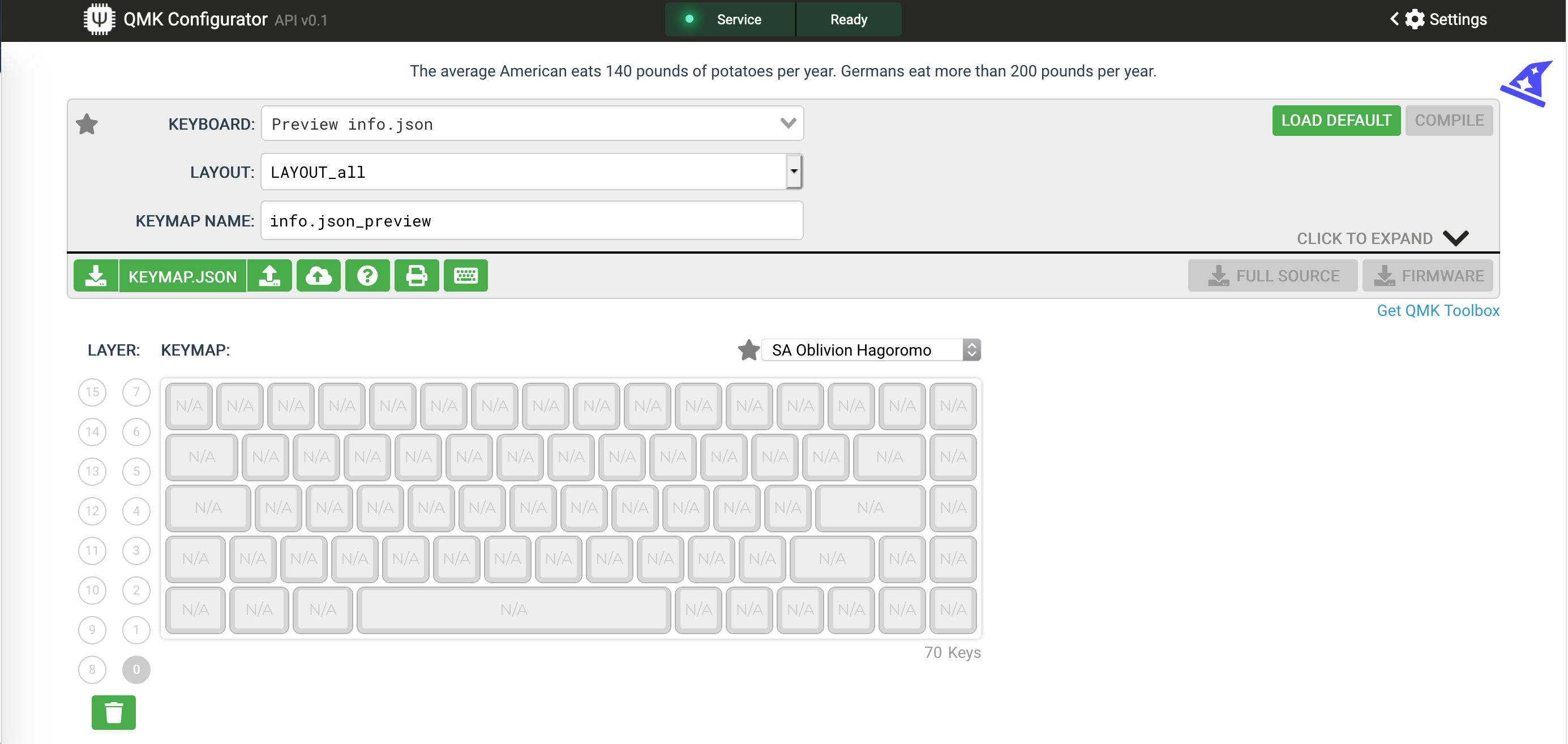
It is possible to try the info.json file by going to the QMK Configurator and enter the Preview Mode by pressing Ctrl+Shift+i. This brings up a file selector window in which it is possible to open our info.json. If all goes well, the configurator will display the keyboard layout without any key label:
Finally, I can try to flash the firmware to the PCB:
- Connect the PCB to the computer
- Open QMK Toolbox
- Press the Keyboard reset button (if not already in DFU mode)
- QMK Toolbox will notice a DFU keyboard is connected by displaying
*** Atmel DFU device connected - Load the firmware that was just built
- Choose the
ATMega32U4microcontroller - Press the flash button
You should see something like this:
*** Attempting to flash, please don't remove device
>>> dfu-programmer atmega32u4 erase --force
    Erasing flash...  Success
    Checking memory from 0x0 to 0x6FFF...  Empty.
>>> dfu-programmer atmega32u4 flash --force /path/to/qmk_firmware/masterzen_aek67_default.hex
    0%                            100%  Programming 0x3F00 bytes...
    [>>>>>>>>>>>>>>>>>>>>>>>>>>>>>>>>]  Success
    0%                            100%  Reading 0x7000 bytes...
    [>>>>>>>>>>>>>>>>>>>>>>>>>>>>>>>>]  Success
    Validating...  Success
    0x3F00 bytes written into 0x7000 bytes memory (56.25%).
>>> dfu-programmer atmega32u4 reset
*** AtmelDFU device disconnected
At this point your computer should recognize that a new keyboard has been connected. If you press any switches it should produce a letter.
You can now test the keyboard and the keymap with the QMK Keyboard Tester. To do so, while the PCB is connected to the computer, use the tweezer to make contact between the two pins of each switch:
If the PCB and keymap are working correctly, the keyboard tester should display the key as registered:
And voila, I now have a fully functional keyboard PCB!
What’s cooking next
And I think that episode concludes the series about keyboard PCB. I’ll expand soon the series of posts to talk about designing a nice case for the PCB.
I hope to be able to cover at least the following:
- plate design
- case design
- selecting screws and nuts
- 3D renders
- technical plans
- fabrication
- prototype assembly
Thanks for following, and stay tuned for the next episodes!
Comments